Chapter 29The Full Architecture and Its Budgets
Every chapter so far has answered one budget question. This chapter puts the answers together on one chip.
- assemble the noise, CMRR, power, area and data-rate budgets of Open-BioAFE;
- choose SAR or ΔΣ per mode;
- add the optional bioimpedance channel;
- clock the whole chip from one reference;
- draw the top-level floorplan, the test chip and its pinout.
Does the assembled Open-BioAFE chip meet every number of its specification (Table 1.2), and where is the margin?
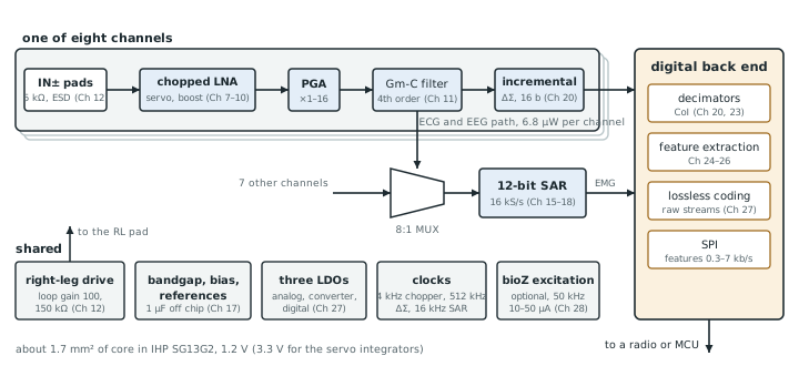
Figure 1.1 drew the signal chain before any block was designed. Twenty-seven chapters later every block has a design, a number and a reason. This chapter adds the numbers up. The figure script figsrc/ch29_figs.py holds the budgets in two tables, so they can be updated as the lab results replace the chapter estimates. Figure 29.1 shows the chip that the budgets describe.
29.1Noise budget
Noise sources add in power. Over the 0.5–100 Hz EEG band, referred to the electrodes:
- the electrodes’ own thermal noise: 0.34 µVrms (wet) or 1.20 µVrms (dry) for the pair (Chapter 3);
- the chopped LNA, including the noise gain of its input, feedback, gate and servo capacitors: 0.36 µVrms (Chapter 10);
- two 5 kΩ input-protection resistors: 0.13 µVrms (Chapter 12);
- the anti-alias filter’s \(kT/C\), divided by the gain of 800 in front of it: 0.05 µVrms (Chapter 11);
- the PGA, divided by the LNA’s gain: 0.02 µVrms;
- the 16-bit ΔΣ converter, divided by the total gain: 0.006 µVrms (Chapter 20).
With wet electrodes: \(\sqrt{0.34^2 + 0.36^2 + 0.13^2 + 0.05^2 + 0.02^2} =\) 0.51 µVrms, a third of the 1.5 µVrms target. With dry electrodes: 1.26 µVrms, 16 % below the target (Figure 29.3a).
With dry electrodes the electrodes themselves take 91 % of the noise power, and the electronics only 9 %. Further front-end current would buy almost nothing; the excess noise of real dry electrodes (Chapter 3) is the real risk to the margin.
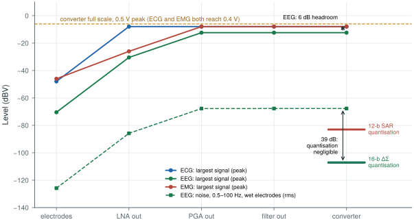
Figure 29.2 follows the largest signal and the noise through the chain. Each mode’s gain brings its largest signal close to the converter’s 0.5 V full scale: 4 mV of ECG through a gain of 100 and 5 mV of EMG through 80 both reach 0.4 V, and 300 µV of EEG through 800 reaches 0.24 V, 6 dB below full scale. The EEG noise rises with the signal, so their ratio is fixed at the electrodes and the LNA and never improves afterwards. By the converter the 0.51 µVrms has become about 0.41 mVrms, 39 dB above the 16-bit converter’s quantisation noise of 4.4 µVrms: the stages after the LNA, the converter included, add almost nothing. That is what the gain plan of Chapter 11 was for.
figsrc/ch29_figs.py.29.2CMRR budget
The channel’s CMRR has an intrinsic part and a part lost to the source (Chapter 7). Chopping lifts the intrinsic CMRR of the capacitively coupled LNA above 100 dB (Chapter 9). Positive-feedback boosting raises the input impedance to about 200 MΩ (Chapter 10). The right-leg drive, with a loop gain of 100 at 50 Hz, divides the common mode at the electrodes by 101 (Chapter 12). In the 10 Vrms CMRR test of the ECG standards (Chapter 4) the residual is 0.06 mVpp, 24 dB inside the 1 mVpp limit. The common-mode input impedance the test requires falls from 1.15 GΩ without the right-leg drive to about 12 MΩ with it, which closes the open design point of Chapter 4. Table 1.2 now states the requirement in that form.
29.3Power, area and data rate
Power. Per channel (Figure 29.3b): the LNA’s 2 µA (2.4 µW), the ΔΣ converter (1.9 µW, in ECG/EEG mode), the PGA (0.6 µW), a share of the right-leg drive, bias and LDOs (0.6 µW), the 3.3 V servo integrator (0.33 µW), choppers and ripple loop (0.3 µW), impedance boosting (0.3 µW), feature extraction and decimation (0.3 µW), and the filter and SAR shares. That totals 6.8 µW in ECG/EEG mode and 4.9 µW in EMG mode, against the 10 µW target: about 3 µW of margin, all of it estimate until the labs measure the blocks.
Area. The input capacitors dominate: two 20 pF MIM capacitors per channel (0.027 mm²), the anti-alias filter’s capacitors (about 0.03 mm²), the servo and boosting capacitors, the LNA, PGA and ΔΣ transistors. With routing, about 0.14 mm² per channel, 1.15 mm² for eight. The SAR, references, bias, LDOs and right-leg drive add about 0.2 mm², the digital back end about 0.3 mm²: about 1.7 mm² of core, plus the pad ring.
Data rate. Features, 0.3–7 kb/s; raw data on demand up to 192 kb/s (eight channels of EMG), both well within an SPI link at a few megahertz (Chapter 27).
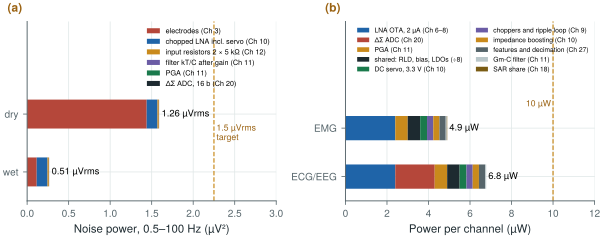
figsrc/ch29_figs.py.The demo below holds the two budgets of Figure 29.3. Change the LNA current, the electrodes and the mode, and watch which term limits which budget.
29.4SAR or ΔΣ per mode
Table 29.1. The Open-BioAFE specification against the designed chain.
| Parameter | Target (Table 1.2) | Designed | Chapters |
|---|---|---|---|
| Input noise, 0.5–100 Hz | < 1.5 µVrms | 0.51 µVrms (wet), 1.26 µVrms (dry) | 3, 6, 9–12 |
| CMRR test residual | < 1 mVpp (≈ 89 dB) | 0.06 mVpp (24 dB margin) | 4, 7, 10, 12 |
| Electrode offset | ±300 mV | ±300 mV with the 4 pF, 3.3 V servo loop | 10 |
| Input impedance | ≥ 2.5 MΩ; ≥ 100 MΩ for dry | 6.25 MΩ chopped; about 200 MΩ boosted | 9, 10 |
| ECG/EEG converter | 16 bits | incremental ΔΣ, 16.5 bits at 500 S/s | 13, 19, 20 |
| EMG/spike converter | 12 bits | asynchronous SAR, ENOB ≥ 11, 16 kS/s shared | 13–18 |
| Power per channel | < 10 µW | 6.8 µW (ECG/EEG), 4.9 µW (EMG) | 6, 14, 18, 20, 29 |
| Supply, process | 1.2 V, SG13G2 | 1.2 V core, 3.3 V servo, IHP SG13G2 | 5, 10, 30 |
| Data out | SPI | features 0.3–7 kb/s; raw ≤ 192 kb/s | 27 |
The converter routing of Figure 1.1 follows from Part III. ECG and EEG go to the incremental ΔΣ: their dynamic range, set by the residual electrode offset and artefacts, needs 16 bits, and at that resolution the oversampled converter’s 1.1 pF sampling capacitor beats the 150 pF a Nyquist converter would need (Chapter 14). EMG and spikes go to the SAR: 12 bits suffice (Chapter 13), and at those bandwidths a shared Nyquist converter at about 12 pJ per conversion is almost free. A heart-rate-only mode could go further, with the ΔΣ at about 8 bits and the front-end bias halved (Chapter 24).
29.5The bioimpedance channel
The optional impedance channel of Chapter 28 adds a balanced current source at about 50 kHz (10–50 µA into the body, from a few microamperes of supply current), square-wave IQ demodulators on the recording channels, and two slow outputs per channel for the SAR. It shares the electrodes with the ECG by frequency separation, and its clock is derived from the same source as the chopper’s. It adds of the order of 5 µW to the chip when running, and is duty-cycled while the contacts are stable.
29.6One clock
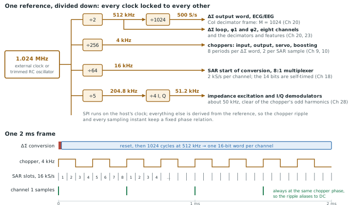
Every clock on the chip comes from one 1.024 MHz reference, an external clock or a trimmed RC oscillator, through dividers (Figure 29.4). Divided by two, it runs the ΔΣ loops, the decimators and the features at 512 kHz; 1024 of those cycles make one incremental conversion, so each channel delivers a 16-bit word every 2 ms, 500 S/s (Chapter 20). Divided by 256, it gives the 4 kHz chopper clock (Chapter 9): a whole number of chopper periods, eight, fits in each ΔΣ conversion. Divided by 64, it starts a SAR conversion every 62.5 µs; the 8:1 multiplexer visits each channel every 500 µs, 2 kS/s per channel, while the SAR times its own bit cycles (Chapter 18). The impedance excitation, 51.2 kHz in I and Q phases, falls between the chopper’s odd harmonics, as Chapter 28 requires. Only the SPI port runs on the host’s clock.
Locking every clock to one reference is what makes the chopper harmless to the converters. Each channel is sampled at the same point of every chopper period, so the residual ripple aliases to a small constant offset instead of a beat tone inside the signal band. A separate oscillator for any one block would bring the beat back, at a frequency that drifts with temperature.
29.7Floorplan
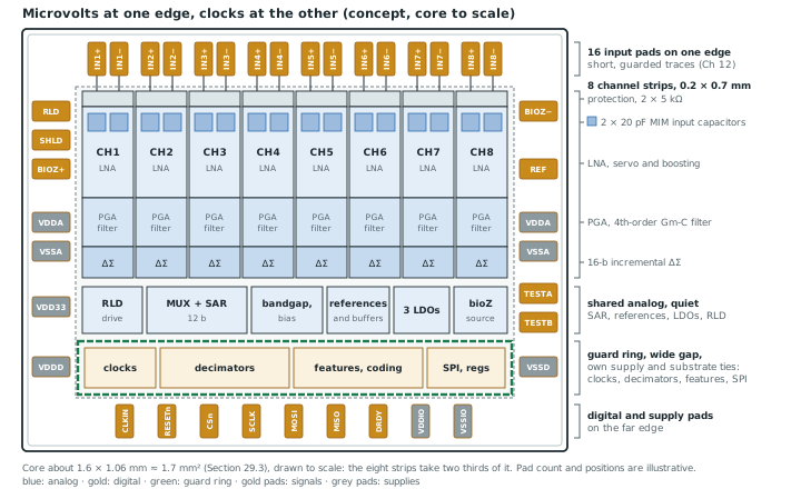
Signal flow decides the floorplan. The eight channels form a row along the edge with the input pads, each channel a strip running from its pads inward: protection, LNA, PGA and filter, then its ΔΣ converter. The input pads and their routing are short and guarded (Chapter 12). The SAR, the bandgap, bias, references and LDOs sit in the middle. The digital back end, which holds the decimators, features and SPI, sits at the opposite edge on its own supply and substrate ties, with a guard ring and a wide gap between it and the analog row. The verdict of the Verma et al. SoC [25] and of the readout architectures in Yazicioglu, Van Hoof and Puers [8] is the same: keep the clocks and the digital switching currents physically and electrically away from the microvolt inputs.
Figure 29.5 draws the floorplan with the core to scale. The eight strips take two thirds of the 1.7 mm², and the two input capacitors alone a fifth of each strip, which is why the capacitor sizes of Chapter 10 set the chip’s area.
29.8Test chip and package
The first silicon is a test chip: the product’s blocks plus the access needed to measure each one (Figure 29.6). An analog test multiplexer brings any LNA, PGA or filter output of any channel to two test pads, so the analog chain can be measured without the converters. Test modes over SPI stream the raw ΔΣ bit streams and SAR codes past the decimators and features, so the converters can be measured without the digital filters, and an on-chip resistor calibrates the impedance channel (Chapter 28). A test-signal generator and the lead-off currents of Chapter 12 let the chip check its own channels. The bench of Chapter 22 supplies the rest: an electrode simulator with its offset, a precision DAC that plays recorded biosignals into the inputs, the CMRR fixture, an FPGA on the SPI port and a separately measured current on every supply.
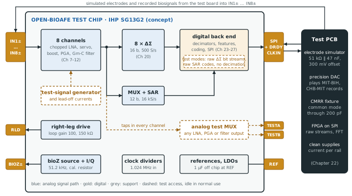
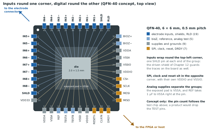
Figure 29.7 puts the test chip’s 40 signals into a 6 × 6 mm QFN-40 package with the floorplan’s rule. The sixteen inputs, two shield pins and the right-leg drive wrap round one corner; SPI, clock and reset sit in the opposite corner on their own I/O supply; the analog supplies separate the two groups, and the exposed pad is the analog ground. On the test board the input corner faces the electrode connector and the digital corner the FPGA, so no microvolt trace runs beside a clock. Plan the pins with the bench, before tape-out (Chapter 30).
On paper the assembled chain meets every target. Noise is 0.51 µVrms with wet electrodes and 1.26 µVrms with dry ones, the CMRR test passes with 24 dB of margin, and the power is 6.8 µW per channel. The margins sit in different places: noise is tight only with dry electrodes, and there the electrodes dominate; CMRR has plenty; power has 3 µW, all of it estimate. Replace each estimate with a lab measurement as the labs are done, and keep the budget tables in figsrc/ch29_figs.py up to date.
Eight channels, each: protected inputs, chopped capacitively coupled LNA with servo loop and impedance boosting, PGA, fourth-order Gm-C filter, second-order incremental ΔΣ. Shared: 12-bit asynchronous SAR, right-leg drive, bandgap, references with an off-chip reservoir capacitor, three LDOs, optional impedance excitation, digital features and SPI. About 1.7 mm² of core in IHP SG13G2.
Treating a budget built from estimates as a result. Every number in Figure 29.3 comes from a chapter’s model, not from a measured circuit; the labs exist to replace them. Keep the source of every entry next to its value, and expect the first silicon to move several of them.
Edit the NOISE and POWER tables in figsrc/ch29_figs.py with your own lab results (Labs 4, 5, 7, 8 and 10) and regenerate Figure 29.3. Then try a heart-rate-only mode: halve the LNA current, drop the ΔΣ, and recompute the noise and power.
Read with this chapter. Verma et al. [25], Yazicioglu, Van Hoof and Puers [8].
- Noise: 0.51 µVrms (wet) and 1.26 µVrms (dry) against 1.5 µVrms; with dry electrodes the electrodes take 91 % of the noise power.
- CMRR: chopping, boosting and a right-leg drive of loop gain 100 pass the ECG test with 24 dB of margin; the common-mode impedance requirement is about 12 MΩ with the right-leg drive.
- Power: 6.8 µW per channel in ECG/EEG mode and 4.9 µW in EMG mode, against 10 µW.
- About 1.7 mm² of core; features 0.3–7 kb/s over SPI.
- One 1.024 MHz reference clocks everything, so the chopper ripple aliases to a constant; floorplan and pinout keep the inputs and the digital at opposite edges.
- ECG/EEG to the incremental ΔΣ, EMG/spikes to the shared SAR, as Part III’s budgets require.