Chapter 15Sample-and-Hold Circuits and Switches
The sampling switch and capacitor set the noise floor of a SAR converter before a single comparison is made.
- derive \(kT/C\) noise and the minimum sampling capacitance per bit;
- size a switch for settling within the acquisition time;
- reduce charge injection and clock feedthrough with bottom-plate sampling;
- design a bootstrapped switch for a 1.2 V supply;
- handle leakage at very low sample rates and multiplexer crosstalk.
How large must the sampling capacitor be, and how should the switch be built, for 12 bits at 1.2 V and a few kilosamples per second?
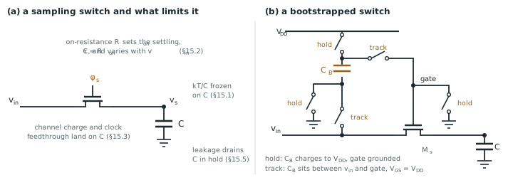
A SAR converter begins every conversion by sampling: a switch connects the input to a capacitor, then opens and holds the voltage while the comparator and DAC work through the bits. For the Open-BioAFE SAR the input range is ±0.5 V differential, 1 V in all (Chapter 11), so a 12-bit LSB is 244 µV. Eight channels at 2 kS/s each share the converter, which therefore runs at 16 kS/s, 62.5 µs per conversion. The numbers below come from SG13G2 simulations in labs/spice/sg13_switch.py; Figure 15.1 shows the switch and the effects that limit it.
15.1kT/C noise and capacitor size
The switch’s thermal noise is frozen on the capacitor when it opens, with variance \(kT/C\) (Chapter 6). In a differential sampler both capacitors contribute, so the differential noise is \(2kT/C\). To keep it below the quantisation noise \(\Delta^2/12\):
For 12 bits over 1 V, \(C_\mathrm{s} \ge 24 \times 4.14\times10^{-21}/(244\ \text{µV})^2 = 1.7\) pF per side. That is a modest capacitor, and as section 15.5 shows, leakage, not noise, will make it larger.
15.2Settling and on-resistance
The capacitor charges through the switch’s on-resistance with time constant \(\tau = R_\mathrm{on}C_\mathrm{s}\). To settle within half an LSB of a full-scale step takes \((N+1)\ln2 \approx 9\tau\) for 12 bits. With an acquisition time of 1 µs and 4 pF, \(R_\mathrm{on}\) must stay below 28 kΩ over the whole input range.
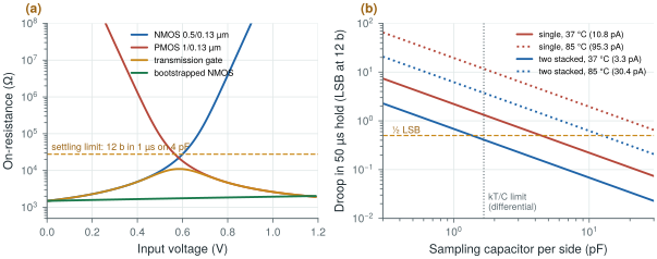
That is a loose requirement at biosignal rates, and the question is only whether the switch stays on at all. Figure 15.2a shows the SG13G2 options at 1.2 V:
- an NMOS (0.5/0.13 µm) is 1.5 kΩ at 0 V but 28 kΩ at 0.6 V, and switches off above about 0.8 V, because its gate overdrive vanishes;
- a PMOS does the opposite;
- a transmission gate (both in parallel) covers the range, with a peak of 11 kΩ at mid-supply, but its resistance, and so its charge injection and distortion, varies with the input;
- a bootstrapped NMOS, whose gate is held at the input voltage plus 1.2 V, stays between 1.5 and 2.0 kΩ everywhere: \(\tau = 8\) ns on 4 pF.
15.3Charge injection and clock feedthrough
When the switch opens, the charge in its channel, about \(C_\mathrm{gg}(V_\mathrm{GS} - V_\mathrm{T})\), leaves through its two terminals, and roughly half lands on the sampling capacitor. The gate–drain overlap capacitance also couples the falling clock edge onto it.
The simulated gate capacitance of the on switch is 0.98 fF, so its channel holds about 0.9 fC. Half of that on 1 pF is 0.44 mV, 1.8 LSB; on 4 pF it is 0.11 mV, 0.45 LSB. In a bootstrapped switch \(V_\mathrm{GS}\) is constant, so the injected charge is nearly independent of the input: it is an offset, not distortion.
Two techniques remove most of what remains. Differential sampling makes the injected charge common to both sides, where the comparator rejects it. Bottom-plate sampling opens a switch at the capacitors’ bottom plate, at a fixed potential, slightly before the input switch. The bottom-plate switch’s charge does not depend on the input, and once it is open the capacitor’s charge can no longer change, so the input switch’s charge has nowhere to go.
15.4Bootstrapped switches
A bootstrapped switch charges a capacitor to \(V_\mathrm{DD}\) during the hold phase and, during sampling, connects it between the switch’s source and gate, so the gate rides at \(V_\mathrm{in} + V_\mathrm{DD}\). Five or six small transistors do the steering. The design rule in SG13G2 is reliability: the thin-oxide 1.2 V devices may see no more than about 1.2 V (plus a margin) across any pair of terminals, although the gate node reaches 2.4 V with respect to ground. Each device in the circuit is arranged so that its terminal differences stay within \(V_\mathrm{DD}\); check this in a transient simulation over all corners, not just at the operating point. The bootstrap capacitor must be several times larger than the switch’s gate capacitance, or charge sharing lowers the boosted voltage. With a 1 fF switch gate, 50 fF is ample.
15.5Leakage and multiplexing
The SG13G2 low-voltage devices have a low threshold voltage, so even with its gate at 0 V a minimum switch carries a subthreshold current. With 0.6 V across it, the simulated 0.5/0.13 µm NMOS leaks 6.5 pA at 27 °C, 10.8 pA at 37 °C and 95 pA at 85 °C. Two devices in series cut that by a factor of three (3.3 pA at 37 °C), because the middle node rises and gives the upper device a negative gate–source voltage.
During the 50 µs a conversion lasts, a leakage \(I\) moves the held voltage by \(I \cdot 50\ \text{µs}/C_\mathrm{s}\) (Figure 15.2b). With a single switch at 37 °C on the 1.7 pF that \(kT/C\) allows, the droop is 1.3 LSB. With two stacked switches on 4 pF it is 0.17 LSB at 37 °C, but 1.6 LSB at 85 °C. Differential sampling cancels the part of the droop that is common to both sides, so what matters is the mismatch of the two leakages, typically a fraction of either. For the 85 °C qualification corner, a larger capacitor, a longer switch or a small negative gate bias in the off state restores the margin.
Multiplexing eight channels into one sampler adds crosstalk. After a conversion the sampling capacitor still holds the previous channel’s voltage, and part of it remains after the next acquisition if the settling is incomplete. With \(\tau = 8\) ns and a 1 µs acquisition, 125 time constants pass and the residue is negligible. The coupling through the off switches’ capacitance into the held voltage, and the kickback of the comparator (Chapter 16) into the multiplexer, are the remaining paths, and both are reduced by a buffer or a precharge phase between channels.
At a few kilosamples per second, settling is not the problem: a bootstrapped NMOS of minimum size settles 12 bits in under 100 ns. \(kT/C\) asks for 1.7 pF per side. Leakage asks for more: the low-threshold SG13G2 switch leaks picoamperes at body temperature and nearly 100 pA at 85 °C, so stack the off devices and use about 4 pF. Sample differentially and on the bottom plate, so charge injection and common droop cancel. Check every node of the bootstrapped switch against the 1.2 V oxide limit.
SAR sampler: differential, bottom-plate, bootstrapped NMOS input switches (0.5/0.13 µm, two stacked in the off path), 4 pF per side (the CDAC of Chapter 17), 1 µs acquisition at 16 kS/s for eight channels. Droop ≤ 0.2 LSB at 37 °C.
Simulating leakage with the simulator’s defaults. The default \(g_\mathrm{min}\) adds \(10^{-12}\) S across each junction, a picoampere at 1 V, the same size as the leakage you want to see; and the default absolute tolerance hides it too. Lower both, as labs/spice/sg13_switch.py does, and simulate at the hottest corner you must meet.
Lab 8 builds the SAR, starting with its bootstrapped sample-and-hold. Run labs/spice/sg13_switch.py, add a hold capacitor and a transient, and measure the droop and the charge injection yourself at 27 and 85 °C.
Read with this chapter. Pelgrom [9] (sample-and-hold circuits), Razavi [13] (switched-capacitor circuits), the IHP Analog Academy SAR module [23].
- Differential \(kT/C\) needs \(C_\mathrm{s} \ge 24kT/\Delta^2\): 1.7 pF per side for 12 bits over 1 V.
- At biosignal rates settling is easy; a bootstrapped NMOS is 1.5–2 kΩ across the range and settles in tens of nanoseconds.
- A plain NMOS or PMOS switch turns off over half the range at 1.2 V; a transmission gate works but varies; bootstrapping keeps \(V_\mathrm{GS}\) and the injected charge constant.
- Charge injection of the minimum switch is about 0.9 fC (1.8 LSB on 1 pF); differential, bottom-plate sampling cancels most of it.
- SG13G2 low-threshold switches leak 6.5 pA (27 °C) to 95 pA (85 °C); stacking and 4 pF keep the 50 µs droop to 0.17 LSB at body temperature.