Chapter 8The AC-Coupled Biopotential LNA
Two capacitors, two pseudo-resistors and an OTA: the Harrison amplifier is the circuit every neural and ExG front-end is compared with.
- derive the gain, band edges and noise of the capacitive-feedback LNA;
- explain how MOS-bipolar pseudo-resistors reach high-pass corners in the millihertz range;
- design the OTA (folded cascode or current-scaled telescopic) for a given noise and bandwidth;
- budget gain, bandwidth and noise for ECG, EEG and EMG modes;
- recognise the linearity, leakage and PVT problems of pseudo-resistors.
How do you size the capacitors, pseudo-resistors and OTA so that one AC-coupled LNA meets the noise, bandwidth and power targets of every Open-BioAFE mode?
Chapter 7 chose a capacitively coupled instrumentation amplifier. This chapter builds its unchopped core, the low-noise amplifier introduced by Harrison and Charles [15], in SG13G2. The numbers come from the device data of Chapter 5 and from two extra simulations in labs/spice/sg13_lna.py: the current–voltage curves of pseudo-resistors and the gate capacitance of the input devices. Chapter 9 then adds the choppers.
8.1The Harrison topology
A fully differential OTA has an input capacitor \(C_1\) in series with each input and a feedback capacitor \(C_2\) from each output back to its input. Across each \(C_2\) sits a pseudo-resistor \(R_\mathrm{pr}\) of teraohms, which sets the DC level of the OTA’s inputs without loading the signal (Figure 8.1). Three numbers describe the response:
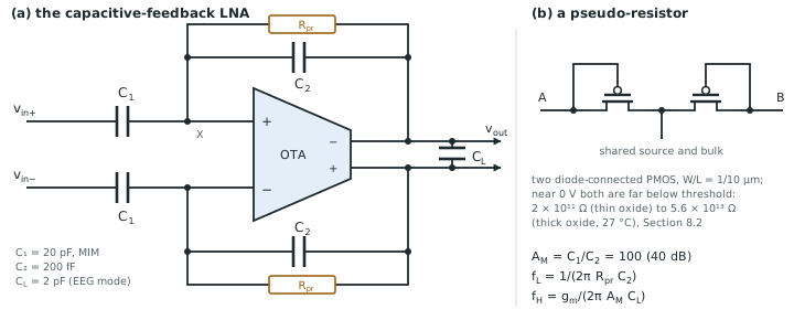
The midband gain is a capacitor ratio. Below \(f_\mathrm{L}\) the pseudo-resistor takes over from \(C_2\) and the gain falls, which removes the electrode offset and slow drift. Above \(f_\mathrm{H}\) the OTA, whose transconductance \(g_\mathrm{m}\) drives the load \(C_\mathrm{L}\) with a loop gain of \(1/A_\mathrm{M}\), runs out of bandwidth. Harrison and Charles’s original amplifier covered 0.025 Hz to 7.2 kHz with 2.2 µVrms of input noise from 80 µW [15].
Use the capacitors of Chapter 7: \(C_1 = 20\) pF and \(C_2 = 200\) fF give \(A_\mathrm{M} = 100\) (40 dB). With 1 µA in each input transistor at \(g_\mathrm{m}/I_\mathrm{D} = 30\) V⁻¹, \(g_\mathrm{m} = 30\) µS, and
\[f_\mathrm{H} = \frac{30\ \text{µS}}{2\pi \times 100 \times C_\mathrm{L}} = 24\ \text{kHz for } C_\mathrm{L} = 2\ \text{pF}, \quad 4.8\ \text{kHz for } 10\ \text{pF}.\]That is far wider than the 100 Hz of an EEG, and on purpose: a chopped amplifier must pass the chopping frequency (Chapter 9). The signal band is cut later, by the filters of Chapter 11 and the converter’s decimation filter.
8.2Pseudo-resistors
A high-pass corner below 0.5 Hz with \(C_2 = 200\) fF needs \(R_\mathrm{pr} > 1/(2\pi \cdot 0.5 \cdot 200\ \text{fF}) = 1.6\) TΩ. A polysilicon resistor of that value would cover a square centimetre. Harrison’s answer is the MOS-bipolar pseudo-resistor: two diode-connected PMOS transistors in series and in opposite directions, each with its bulk tied to the shared source. For small voltages of either sign one device is a subthreshold MOSFET with almost no gate drive and the other a reverse-biased diode, so the current is femtoamperes to picoamperes.
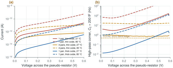
labs/spice/sg13_lna.py simulates back-to-back pairs of \(W/L = 1/10\) µm PMOS devices (Figure 8.2). The small-signal resistance at 20 mV and the corner with \(C_2 = 200\) fF are:
- one thin-oxide pair: \(2\times10^{11}\) Ω, \(f_\mathrm{L} = 4.1\) Hz at 27 °C; \(1.2\times10^{10}\) Ω, 68 Hz at 85 °C;
- four thin-oxide pairs in series: \(7.6\times10^{11}\) Ω, 1.05 Hz at 27 °C, almost independent of voltage; 17.5 Hz at 85 °C;
- one thick-oxide pair (the 3.3 V devices): \(5.6\times10^{13}\) Ω, 0.014 Hz at 27 °C and 0.032 Hz at 37 °C; \(7.7\times10^{11}\) Ω, 1.0 Hz at 85 °C.
The thin-oxide devices of SG13G2, with their low threshold, leak too much: a single pair puts the corner at 4 Hz, inside every ExG band. The thick-oxide pair reaches the millihertz range at body temperature.
ngspice adds a conductance \(g_\mathrm{min}\), \(10^{-12}\) S by default, across junctions to help convergence. That is a 1 TΩ resistor in parallel with each device, the same size as the pseudo-resistor you are trying to simulate. With the default the thick-oxide pair above simulates at \(1.9\times10^{12}\) Ω, exactly \(2/g_\mathrm{min}\), thirty times too low. Simulate pseudo-resistors with .option gmin=1e-15 abstol=1e-15 and check that the result does not move when \(g_\mathrm{min}\) falls further.
8.3OTA design
The OTA sets the noise, and almost all of its noise should come from the input pair. Two topologies are common. A folded cascode has a wide output swing, but its folding current sources carry as much current as the input pair and add their own noise, a fraction \(g_\mathrm{m,fold}/g_\mathrm{m,in}\) of it. A current-scaled telescopic OTA stacks the cascodes above the input pair and starves the load branch, so that nearly all the current flows through the input devices. With the loads in strong inversion at 5 V⁻¹ and the inputs at 30 V⁻¹, the loads add 17 % to the noise power (Chapter 6). At 1.2 V the telescopic stack is tight but fits, thanks to the 0.17 V gate-source voltage of the SG13G2 NMOS (Chapter 5).
The capacitive feedback adds a noise penalty of its own. The OTA’s input noise appears at the amplifier input multiplied by the ratio of all the capacitance on the OTA input node to \(C_1\):
\(C_\mathrm{in}\) is the gate capacitance of the OTA’s input device. That puts the input pair in a squeeze. Large devices lower the flicker noise (Chapter 5) but raise \(C_\mathrm{in}\): the simulation gives about 2.2 fF per µm² of gate in weak inversion (2.16 pF for a 100/10 µm NMOS).
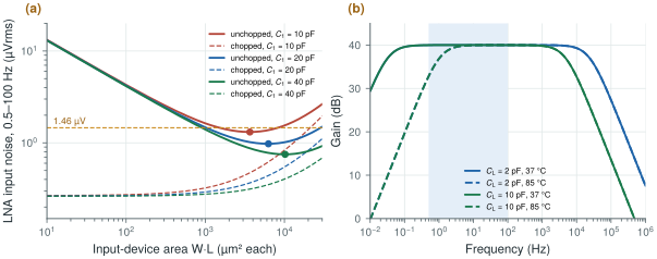
At 1 µA per device and \(C_1 = 20\) pF, sweep the area of each NMOS input device and add the capacitive penalty to the pair noise of Chapter 5 (Figure 8.3a):
- Unchopped, flicker noise falls with area while the penalty grows. The best area is about 6200 µm² per device, where the noise gain is 1.68 and the input noise 0.98 µVrms. With \(C_1 = 10\) pF the optimum is 3600 µm² and 1.31 µVrms; with 40 pF, 10 200 µm² and 0.75 µVrms.
- Chopped, only thermal noise is left, which does not fall with area, so small devices win: 0.27 µVrms at 100 µm² and 0.29 µVrms at 1000 µm².
Chopping therefore cuts the noise by a factor of three to four and lets the input devices shrink by a factor of about sixty.
8.4Gain, bandwidth and noise budget
One LNA must serve three modes whose signals differ by three orders of magnitude (Chapter 2).
ECG and EEG. Signals of tens of microvolts to a few millivolts, the 1.5 µVrms noise target, and a high-pass corner at 0.5 Hz or below (0.05 Hz for diagnostic ECG). A gain of 100 brings the signal to the millivolt level for the next stage.
EMG. Up to 5 mV peak, which at a gain of 100 is 0.5 V peak at the output, beyond the ±0.45 V a 1.2 V stage can swing. Switching \(C_2\) from 200 fF to 2 pF drops the gain to 10 (20 dB) and lowers \(f_\mathrm{L}\) tenfold, which does no harm. The noise target relaxes with the signal.
Input impedance. \(C_1\) also sets the load on the electrodes: 20 pF is 160 MΩ at 50 Hz and 16 MΩ at 500 Hz, per input. That is enough for wet electrodes and marginal for dry ones at EMG frequencies; chopping lowers it further, which Chapter 10 repairs.
Bandwidth. The LNA’s band runs to \(f_\mathrm{H} \approx 5\)–24 kHz depending on its load (Figure 8.3b), but its noise must be counted only over the signal band. That holds only if something removes the rest before the converter samples. Integrated up to 24 kHz with a first-order roll-off, the thermal noise of the chopped pair is about 5 µVrms. Folded into a Nyquist-rate converter it would swamp the 1.5 µVrms target (Chapter 13). The anti-alias filtering of Chapter 11 is part of the noise budget, not an afterthought.
Move the capacitors, the OTA’s transconductance and the pseudo-resistor below and watch the pass band. It starts at this chapter’s design: 20 pF / 200 fF, 2 pF of load, 30 µS and one pair of thin-oxide pseudo-resistors.
8.5Linearity and pseudo-resistor problems
Pseudo-resistors are what make the Harrison amplifier small, and they are its weakest part.
- Voltage dependence. The resistance falls steeply once more than a few hundred millivolts appear across it (Figure 8.2b). A large motion artefact or a stimulation pulse drives the OTA output, and with it the pseudo-resistor, far from its rest point. The corner then jumps from 0.03 Hz to about 1 Hz, and the baseline recovers first quickly, then very slowly. Large EMG signals at the output modulate the corner in the same way, which shows up as low-frequency distortion.
- Temperature and leakage. Every variant loses one to two decades of resistance between 27 and 85 °C, as junction leakage grows. A wearable at skin temperature is fine with the thick-oxide pair; the same chip at 85 °C during a qualification test has its corner at 1 Hz.
- Process. Subthreshold and leakage currents vary by large factors between corners and wafers, so the corner is uncertain by more than a decade.
- Gate leakage of the input devices. The pseudo-resistor also carries the OTA’s input current. A 250/4 µm thin-oxide SG13G2 NMOS, the size the noise calls for, leaks 3–25 pA through its gate at 27 °C, depending on its gate–drain voltage. The thick-oxide pseudo-resistor carries only 0.35 pA even with 0.6 V across it, so the leakage pushes the OTA’s input hundreds of millivolts away from its output and the amplifier saturates. An unchopped LNA with a teraohm bias therefore needs thick-oxide input devices, which leak about 10⁻²⁰ A but have about 2.7 times the flicker-noise power (Lab 4). A chopped LNA escapes the problem: the signal at the OTA’s input sits at the chopping frequency, so the input node can be biased through about 10 GΩ, where 3 pA costs only 30 mV (Chapter 10).
Three alternatives trade area or power for control. A bias-controlled pseudo-resistor drives the gates from a replica circuit that holds a set current, which fixes the resistance against temperature and process. A duty-cycled resistor connects an ordinary resistor \(R\) for a fraction \(D\) of each clock period, behaving like \(R/D\). And a DC servo loop (Chapter 10) takes over the job of the pseudo-resistor: an integrator with a well-defined time constant feeds the output’s DC level back to the input, and the pseudo-resistor only biases the nodes.
Set the gain with \(C_1/C_2\), the upper edge with the OTA’s \(g_\mathrm{m}\) and load, and leave the signal band to the filters downstream, which must remove the wideband noise before sampling. In SG13G2 the thin-oxide pseudo-resistors leak too much; use thick-oxide devices, and simulate them with a small \(g_\mathrm{min}\). Check that the OTA’s gate leakage is far below what the pseudo-resistor can carry. Count the input device’s gate capacitance in the noise. Without chopping it forces an optimum of several thousand square micrometres per device; with chopping the devices shrink and the noise falls threefold. Treat the pseudo-resistor’s corner as uncertain by a decade and let a servo loop define it where it matters.
LNA: \(C_1 = 20\) pF, \(C_2 = 200\) fF (gain 40 dB; 2 pF and 20 dB in EMG mode), thick-oxide PMOS pseudo-resistor pair (\(W/L = 1/10\) µm, \(f_\mathrm{L} \approx 0.03\) Hz at 37 °C), OTA with NMOS inputs of 100–1000 µm² at 1 µA each: thin-oxide only when chopped, with the input node biased through about 10 GΩ; thick-oxide in an unchopped LNA, which also needs a folded cascode to hold its output at the input common mode (Section 8.5, Lab 4), \(f_\mathrm{H}\) about 5–24 kHz set by the load. Input noise with chopping about 0.3 µVrms over 0.5–100 Hz.
Lab 4 designs the capacitive-feedback LNA with pseudo-resistors in SG13G2: AC, noise and transient simulations and the NEF versus bias current. Begin with labs/spice/sg13_lna.py: rerun the pseudo-resistors at the ss and ff corners, and at the default \(g_\mathrm{min}\) to see the trap above for yourself.
Read with this chapter. Harrison and Charles [15], Yazicioglu, Van Hoof and Puers [8].
- Gain \(C_1/C_2\), low corner \(1/(2\pi R_\mathrm{pr}C_2)\), high corner \(g_\mathrm{m}/(2\pi A_\mathrm{M}C_\mathrm{L})\): 40 dB from 20 pF and 200 fF, and 5–24 kHz from 30 µS.
- SG13G2 thin-oxide pseudo-resistors give only \(10^{11}\)–\(10^{12}\) Ω; a thick-oxide pair gives \(5.6\times10^{13}\) Ω (0.03 Hz at 37 °C) but falls to about 1 Hz at 85 °C or with 0.45 V across it.
- The default \(g_\mathrm{min}\) of a simulator caps a teraohm simulation; lower it.
- The OTA’s noise reaches the input multiplied by \((C_1+C_2+C_\mathrm{in})/C_1\); with about 2.2 fF/µm² of gate capacitance this sets an optimum input-device size without chopping (0.98 µVrms at 6200 µm²) and favours small devices with it (0.27–0.29 µVrms).
- The LNA’s wide band must be filtered before sampling, or its integrated noise, about 5 µVrms, folds into the signal band.