Chapter 7Instrumentation Amplifier Architectures
The instrumentation amplifier is where the common-mode rejection of the whole chain is won or lost.
- analyse the three-op-amp, current-feedback and capacitively coupled instrumentation amplifiers (CCIA);
- trace where CMRR comes from in each: resistor or capacitor mismatch, finite common-mode gain, input impedance;
- design for a rail-to-rail common-mode range at a 1.2 V supply;
- choose an IA architecture for the Open-BioAFE channel.
Which instrumentation-amplifier architecture gives more than 90 dB of CMRR and a ±300 mV offset range at microwatt power and 1.2 V?
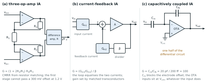
An instrumentation amplifier (IA) amplifies the difference between two inputs and ignores what they have in common. For a biopotential channel that means amplifying a microvolt ECG or EEG while rejecting the millivolts to volts of mains common mode of Chapter 4, and tolerating up to ±300 mV of electrode offset (Chapter 3). Three architectures dominate (Figure 7.1). This chapter compares them on CMRR, offset range and power, all at 1.2 V.
7.1The three-op-amp instrumentation amplifier
The textbook IA has two stages [7]. Two non-inverting op-amps, cross-connected through a gain resistor \(R_1\) and two feedback resistors \(R_2\), form the first stage. A difference amplifier of gain \(G_2 = R_4/R_3\) follows:
\[G_1 = 1 + \frac{2R_2}{R_1}, \qquad G_\mathrm{dm} = G_1\,G_2.\]The first stage passes a common-mode input with a gain of exactly one, because no current flows through \(R_1\) when both inputs move together. All the common-mode rejection happens in the difference amplifier, and that stage rejects common mode only as well as its four resistors match. If they are off by a tolerance \(t\), its worst-case CMRR is [16]
The first stage multiplies the second stage’s CMRR by its own gain, because it amplifies the difference and not the common mode. That is why the gain goes into the first stage.
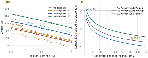
With 0.1 % resistors and \(G_2 = 1\), the worst case is \(2/(4 \times 0.001) = 500\), or 54 dB. A Monte Carlo run with the resistors spread uniformly over ±0.1 % gives a median of 67.7 dB (Figure 7.2a), so typical parts do better than the worst case, but not by enough.
A first-stage gain of 100 lifts the worst case to 94 dB and the median to 108 dB. With \(G_1 = 1.5\) the median is only 71 dB. CMRR therefore depends on how much gain can be put in front of the difference amplifier.
At 1.2 V that gain is the problem. The first stage is DC-coupled, so it amplifies the electrode offset along with the signal. With ±300 mV of offset and about ±0.45 V of output swing, the first stage can have a gain of at most \(0.45/0.3 = 1.5\) (Figure 7.2b). At that gain the IA’s CMRR is the difference amplifier’s, 54–71 dB with 0.1 % resistors, well short of 90 dB. On-chip resistors match to a few tenths of a percent at best, and the two extra op-amps and the resistor string draw current that a 10 µW channel does not have. The classic IA belongs on a circuit board with a ±5 V supply, not in a microwatt 1.2 V chip.
figsrc/ch07_figs.py.7.2Current-feedback (indirect current feedback) IAs
A current-feedback IA replaces the resistor bridge with two matched transconductors. The input transconductor turns the input difference into a current; a second transconductor turns a fraction of the output, set by a resistive divider, into a current that opposes it. The loop forces the two currents to be equal, so the gain is the divider ratio times the ratio of the two transconductances, which are matched by layout.
The key property is that the input transconductor sees only the difference of its two inputs. A common-mode input moves both its gates together and produces no current to first order, so CMRR no longer depends on resistor matching. It is set by the transconductor’s own common-mode rejection, which for a well-designed differential pair with a high-impedance tail is 100 dB or more.
The weakness is input range. A weak-inversion differential pair is linear only over a few times \(nU_T\), some tens of millivolts. Degeneration extends that range at the cost of noise and current, but not to ±300 mV. A current-feedback IA in a biopotential channel therefore needs the electrode offset removed at its input. A DC servo loop feeding back into the input transconductor can do that (Chapter 10), and with chopping, current-feedback IAs reach excellent offset and CMRR. They remain a strong choice for DC-coupled channels where the electrode offset itself carries information.
7.3Capacitively coupled IAs
A capacitively coupled IA puts a capacitor \(C_\mathrm{in}\) in series with each input and a capacitor \(C_\mathrm{fb}\) in each feedback path of a fully differential OTA. The OTA holds its inputs at a virtual ground, so the signal charge that flows through \(C_\mathrm{in}\) must flow through \(C_\mathrm{fb}\):
A very large resistance \(R_\mathrm{fb}\) across each \(C_\mathrm{fb}\), usually a pseudo-resistor of \(10^{11}\)–\(10^{13}\) Ω (Chapter 8), sets the DC operating point and a sub-hertz high-pass corner.
Three properties make this the dominant ExG front-end. First, \(C_\mathrm{in}\) blocks DC: the ±300 mV electrode offset appears across the capacitor and never reaches the OTA, so the OTA’s input common mode can sit wherever its devices like it, and the gain can be 100 in a single stage. Second, the gain is a ratio of two on-chip capacitors, which match far better than resistors and draw no static current. Third, the OTA’s inputs carry no DC current, so the only load on the electrodes is capacitive. The weakness is the input impedance: at 50 Hz a 20 pF capacitor is 160 MΩ, and once the inputs are chopped the impedance falls further (Chapter 9, Chapter 10).
Choose a gain of 100 (40 dB) with \(C_\mathrm{in} = 20\) pF and \(C_\mathrm{fb} = 200\) fF. SG13G2’s MIM capacitors have 1.5 fF/µm² (cap_carea in the PDK), so each input capacitor takes 13 300 µm², about 115 × 115 µm. With \(R_\mathrm{fb} = 10^{12}\) Ω the high-pass corner is \(1/(2\pi \cdot 10^{12} \cdot 200\ \text{fF}) = 0.8\) Hz; \(10^{13}\) Ω brings it to 0.08 Hz, low enough for diagnostic ECG.
The ±300 mV electrode offset sits across \(C_\mathrm{in}\). Amplified by 100 it would be ±30 V; here it produces no output at all.
7.4CMRR mechanisms and mismatch
Two separate mechanisms limit the CMRR of a real channel, and the ECG standards’ test (Chapter 4) catches both.
Intrinsic CMRR is the amplifier’s own, measured with perfectly matched sources. In the three-op-amp IA it is the resistor matching of section 7.1, combined with the op-amps’ CMRR. In a CCIA it is the matching of the two input capacitors: a common-mode voltage \(V_\mathrm{cm}\) pushes a charge \(V_\mathrm{cm}C_\mathrm{in}\) through each one, and if they differ by \(\Delta C\) the difference, \(V_\mathrm{cm}\Delta C\), lands in the feedback capacitors as a differential output. The CMRR is \(C_\mathrm{in}/\Delta C\).
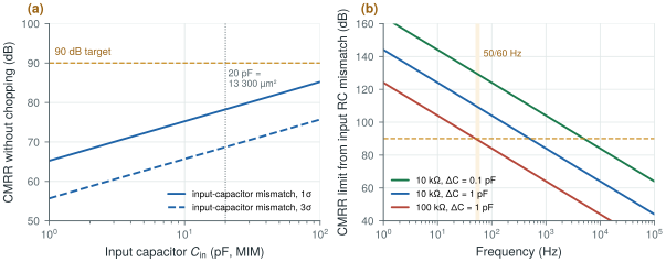
SG13G2’s MIM capacitors match to 1 %·µm. For two 13 300 µm² input capacitors, the difference scatters by \(\sqrt2 \times 1\,\%/\sqrt{13\,300} = 0.012\,\%\), a CMRR of 78 dB at one standard deviation and 69 dB at three (Figure 7.3a). Even 100 pF capacitors stay below 90 dB at one standard deviation. An unchopped CCIA cannot meet the target by matching alone.
The cure is chopping (Chapter 9). An input chopper swaps the two inputs between the two capacitors every half period, so the charge error \(V_\mathrm{cm}\Delta C\) changes sign at the chopping frequency. The output chopper then moves it up to the chopping frequency, where the low-pass filter removes it. What remains is the much smaller mismatch of the chopper switches themselves.
CMRR lost to the source comes from outside the amplifier. The electrode impedances differ, so each input divides the common mode differently against the amplifier’s common-mode input impedance, \(\Delta Z/Z_\mathrm{cm}\) of Chapter 4. Any RC network in front of the inputs, such as protection resistors with their parasitic capacitance, adds a term \(2\pi f R\,\Delta C\) that grows with frequency (Figure 7.3b). With 10 kΩ and 1 pF of imbalance it limits CMRR to 110 dB at 50 Hz, but to 84 dB at 1 kHz. That is why CMRR is specified and checked at 50 and 60 Hz and their harmonics, not at DC, and why Chapter 12 keeps the input filters matched. The effective CMRR of the channel combines both mechanisms:
\[\frac{1}{\mathrm{CMRR_{eff}}} = \frac{1}{\mathrm{CMRR_{int}}} + \frac{\Delta Z}{Z_\mathrm{cm}}.\]Chapter 4 found that with the standards’ 40.7 kΩ imbalance at 50 Hz, 90 dB effective CMRR needs a common-mode input impedance of about 1.9 GΩ. No amount of intrinsic CMRR helps if \(Z_\mathrm{cm}\) is too low. Reducing the body’s common mode with the right-leg drive (Chapter 12) and raising \(Z_\mathrm{cm}\) (Chapter 10) are the two ways out.
figsrc/ch07_figs.py.7.5Common-mode range at 1.2 V
The input common-mode range of an IA must cover the body’s common-mode voltage plus the electrode offset. With a right-leg drive the body sits near the amplifier’s mid-supply, so the range needed is about ±0.3 V around 0.6 V on a 1.2 V supply.
The three architectures handle this very differently. In the three-op-amp IA and the current-feedback IA, the input devices see the electrode voltages directly, so their common-mode range must include the full offset. In a weak-inversion NMOS pair that is easy at the bottom of the range: the SG13G2 NMOS carries 100 nA per square at only 0.17 V of gate-source voltage (Chapter 5). At the top of the range, the tail current source and the load devices run out of headroom. Rail-to-rail input stages with complementary NMOS and PMOS pairs solve this, at the price of a gain and noise change where one pair hands over to the other.
The CCIA avoids the problem: its input capacitors absorb the offset and the body’s common mode, and the OTA’s input common mode is set by its own bias network, independent of the electrodes. At 1.2 V that alone is a decisive advantage.
At 1.2 V with ±300 mV of electrode offset, a DC-coupled first stage can have a gain of only 1.5, which leaves the three-op-amp IA with the CMRR of its resistor matching, 54–71 dB. A current-feedback IA rejects common mode without matched resistors but cannot swallow ±300 mV without a servo loop. A capacitively coupled IA blocks the offset, takes a gain of 100 in one stage from a ratio of MIM capacitors and draws no static input current. Its intrinsic CMRR, about 78 dB from capacitor matching, needs chopping to pass 90 dB, and the channel’s effective CMRR also needs a high common-mode input impedance or a right-leg drive.
Architecture: chopped capacitively coupled IA. \(C_\mathrm{in} = 20\) pF (MIM, 13 300 µm²), \(C_\mathrm{fb} = 200\) fF, gain 40 dB, high-pass corner below 0.5 Hz with pseudo-resistors. Intrinsic CMRR above 100 dB after chopping; effective CMRR above 90 dB with the right-leg drive of Chapter 12.
Quoting the CMRR of the amplifier alone. A data-sheet CMRR of 120 dB says nothing about the channel’s CMRR with real electrodes, which is limited by \(\Delta Z/Z_\mathrm{cm}\). The ECG standards test the whole channel with an imbalanced source; simulate the same way, with the 51 kΩ ∥ 47 nF imbalance in one lead and at 50 and 60 Hz.
figsrc/ch07_figs.py holds the Monte Carlo of the difference amplifier and the capacitor-mismatch model. Change the resistor distribution from uniform to Gaussian, or add a 1 pF parasitic capacitance mismatch at the IA inputs, and watch the CMRR at 50 Hz and at 1 kHz.
Read with this chapter. Yazicioglu, Van Hoof and Puers [8], Pallàs-Areny and Webster [16], Webster [7] (biopotential amplifiers).
- In the three-op-amp IA the first stage multiplies the difference amplifier’s CMRR, about \((1+G_2)/(4t)\), by its gain; with ±300 mV of offset at 1.2 V that gain is at most 1.5, leaving 54–71 dB with 0.1 % resistors.
- A current-feedback IA does not need matched resistors for CMRR, but its input range is tens of millivolts, so the offset must be removed at its input.
- A capacitively coupled IA blocks the offset, sets its gain with \(C_\mathrm{in}/C_\mathrm{fb}\) and needs no matched resistors; at 20 pF its MIM matching gives about 78 dB unchopped, so it is chopped.
- Effective CMRR combines the amplifier’s own with \(\Delta Z/Z_\mathrm{cm}\); RC mismatch at the inputs costs 20 dB per decade of frequency.
- Open-BioAFE uses a chopped CCIA with a gain of 100.