Chapter 17Capacitive DACs and References
The capacitive DAC is the SAR’s sampling capacitor, its subtractor and its reference all at once; its matching sets the linearity and its switching sets much of the energy.
- compare binary-weighted, split (bridge) and C-2C capacitor arrays;
- compute the switching energy of the conventional, monotonic, \(V_\mathrm{cm}\)-based and merged-capacitor schemes;
- size the unit capacitor from matching and from \(kT/C\);
- choose between MOM and MIM capacitors in SG13G2 and lay them out in common centroid;
- design reference buffering and decoupling.
How small can the unit capacitor be for 12-bit linearity, and which switching scheme minimises the DAC energy?
In a charge-redistribution SAR the input is sampled onto an array of binary-weighted capacitors. During conversion the array’s bottom plates are switched between the references one bit at a time, and the comparator watches the floating top plate (Chapter 18). Chapter 15 asked for about 4 pF per side; Chapter 14 showed that 1 % unit mismatch costs 4.5 dB of SNDR at 12 bits. This chapter reconciles the two and chooses the switching scheme.
17.1Capacitor array topologies
Binary-weighted. Bit \(k\) is \(2^k\) unit capacitors, plus one dummy, \(2^N\) units in all. It is the most linear arrangement for a given unit, because every weight is built from identical units, but the total grows as \(2^N\).
Split (bridge). A small bridge capacitor attenuates an LSB sub-array, so a 12-bit array can be built as two 6-bit arrays of 64 units each. The total shrinks by a factor of 30, but the bridge capacitor’s value and the top plate’s parasitic capacitance must be accurate, and every unit of the MSB sub-array now carries 64 LSB of weight, so its mismatch matters 64 times more. Split arrays usually need calibration.
C-2C. A ladder of unit and double-unit capacitors, the capacitive analogue of an R-2R ladder. Its total grows only linearly with \(N\), but parasitics at every node spoil its linearity beyond 8–10 bits.
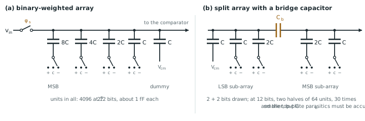
For 12 bits the binary array is the honest choice, provided its unit can be small. Section 17.3 shows how small. Figure 17.1 draws the binary and split arrays.
17.2Switching schemes and energy
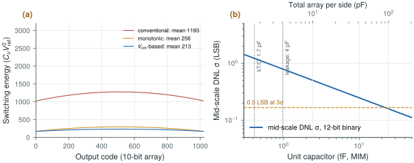
Every conversion charges and discharges parts of the array from the references, and that charge, times the reference voltage, is the DAC’s energy. figsrc/ch17_figs.py computes it by charge conservation on the floating top plate, for every output code, in units of \(C_uV_\mathrm{ref}^2\) (Figure 17.2a):
- Conventional: each bit is first tried by switching its capacitor to \(V_\mathrm{ref}\); if the trial was too high, it is switched back, wasting the charge. Average 1193 at 10 bits, 4777 at 12 bits.
- Monotonic: the input is sampled on the top plates and every step only lowers one side, so no charge is ever thrown away, and the array needs one bit fewer. Average 256 at 10 bits, which matches the 255.5 usually quoted for this scheme, and 1024 at 12 bits. Its drawback is that the common-mode voltage at the comparator falls during the conversion.
- \(V_\mathrm{cm}\)-based (and the closely related merged-capacitor switching): all bottom plates start at mid-reference and move up or down by half a reference, which halves the voltage steps. Average 213 at 10 bits, 853 at 12 bits, with a constant common mode, at the price of a third reference level.
The exact averages depend on conventions, such as whether the sampling phase is counted and how large the array is, so published values differ by tens of percent. The ranking does not.
With 4 pF per side and 4096 units, \(C_u = 0.98\) fF. With \(V_\mathrm{ref} = 1\) V and the \(V_\mathrm{cm}\)-based scheme, each conversion costs \(853 \times 0.98\ \text{fF} \times 1\ \text{V}^2 = 0.84\) pJ, 13 nW at 16 kS/s. The conventional scheme would cost 4.7 pJ.
Compare with the comparator’s 4 pJ per conversion (Chapter 16): with an efficient switching scheme, the DAC is no longer the largest consumer.
17.3Unit-capacitor sizing
Two requirements set the unit capacitor, and they pull in opposite directions.
Noise (\(kT/C\), Chapter 15) sets the total: at least 1.7 pF per side, about 4 pF for leakage margin.
Matching sets the unit. In the binary array the mid-scale step compares the MSB against all the other bits, so its DNL scatters by about \(\sigma_u\sqrt{2^N}\) LSB (Chapter 14):
SG13G2 MIM capacitors have \(A_C = 1\) %·µm and 1.5 fF/µm² (Chapter 5). For a mid-scale DNL within ±0.5 LSB at three standard deviations, \(\sigma_u \le 0.26\) %, which needs 14.8 µm² per unit: 22 fF, and 91 pF per side for the whole array (Figure 17.2b). That is 23 times the noise requirement, and 23 times the switching energy.
The 4 pF array has 0.98 fF units. With MIM matching they would have \(\sigma_u = 1.24\) % and a mid-scale DNL of 0.79 LSB at one standard deviation, so the array will have missing codes unless something corrects it. And 0.65 µm² is only half the smallest MIM capacitor the PDK draws (Section 17.4).
The resolution is to keep the small array and correct its errors digitally: redundant, non-binary weights that tolerate a wrong decision, and a foreground calibration that measures each weight once and stores it (Chapter 18). Matching then has to be good enough only for the redundancy to absorb, which is a factor of several looser.
figsrc/ch17_figs.py.17.4Capacitors in SG13G2
SG13G2 offers two kinds of capacitor. MIM capacitors are a dielectric layer between two dedicated metal plates near the top of the stack: 1.5 fF/µm², 1 %·µm matching, low parasitic capacitance to the substrate, but a minimum size: the PDK’s cmim cell is at least 1.14 × 1.14 µm², about 1.95 fF (Lab 14). A 1 fF unit is therefore below what can be drawn as MIM: it must be a MOM capacitor, or the array must use 1.95 fF units and 8 pF per side, which doubles the switching energy and halves the mismatch. MOM capacitors are interdigitated fingers in the ordinary metal layers (the cap_cmom models): they can be made far smaller, down to a fraction of a femtofarad, at lower density and with matching that must be taken from the PDK’s statistical models and from layout care.
Whichever is used, the layout decides the matching as much as the device does:
- Common centroid: place the units of each bit symmetrically around the array’s centre, so that linear gradients in oxide thickness or temperature cancel;
- Dummy units around the array’s edge, so that every active unit sees the same neighbours;
- Shielded routing: the top-plate node is the comparator input, so keep its wiring short, shielded by a grounded layer below, and keep the parasitic capacitance to the bottom-plate lines equal for every bit.
The IHP Analog Academy SAR module [23] and the JKU SAR design [24] show complete open layouts to learn from.
17.5References
The references deliver the DAC’s switching charge. A charge that arrives late, or a reference that droops while it is delivered, is a conversion error.
At the MSB decision the array draws up to about \(C_\mathrm{DAC}V_\mathrm{ref}/2 = 2\) pC from the reference. Delivered from an on-chip decoupling capacitor of 100 pF, that is a 20 mV droop, which the reference buffer must restore to within half an LSB, 122 µV, before the decision. Each bit of the 16 kS/s converter has about 4.8 µs, so the buffer must settle by a factor of 160 (\(\ln 160 = 5.1\) time constants) in that time: \(\tau \le 0.94\) µs. On 100 pF that needs a transconductance of about 106 µS, roughly 4 µA in weak inversion. Running continuously, that is 4.8 µW, or 300 pJ per conversion at 16 kS/s, fifteen times the converter’s whole energy budget.
The way out is to move the charge reservoir off chip. With a 1 µF capacitor on a reference pin, the MSB’s 2 pC causes a droop of only 2 µV, far below an LSB, and the on-chip buffer has to supply only the average reference current: 0.84 pJ per conversion at 1 V and 16 kS/s is 13 nA. A bandgap and a slow, low-power buffer suffice. The price is one pin and one external capacitor, which a wearable system can afford. Where no pin is available, a reference whose droop is the same for every conversion, so that it calibrates out, or a duty-cycled buffer that runs only during conversions, are the alternatives.
Use a binary array of about 1 fF units, 4 pF per side, sized by noise and leakage, and let redundancy and calibration (Chapter 18) handle the mismatch, which at that size is 0.8 LSB at mid-scale. Switch it with the \(V_\mathrm{cm}\)-based or monotonic scheme: 0.8–1 pJ per conversion instead of 4.7. Lay it out in common centroid with dummies and a shielded top plate. Budget the reference: a fast on-chip buffer would cost fifteen times the converter’s energy, so give the reference an off-chip 1 µF capacitor and let a 13 nA buffer supply the average current.
12-bit binary CDAC, about 1 fF MOM units (the smallest MIM cell, 1.95 fF, would double the array to 8 pF per side), 4 pF per side, \(V_\mathrm{cm}\)-based switching (0.84 pJ per conversion), common-centroid layout with dummies, redundancy and foreground calibration in the SAR logic. Reference: bandgap and low-power buffer (average current about 13 nA) with an off-chip 1 µF decoupling capacitor on the reference pin.
Forgetting the top plate’s parasitic capacitance. It does not add to the weights but to the total, so it attenuates the DAC’s full-scale step at the comparator, and any part of it that depends on the code (for example from routing over bottom-plate lines) adds nonlinearity. Extract the layout (Chapter 30) and simulate the extracted array before trusting a schematic’s DNL.
Add the merged-capacitor scheme to energy() in figsrc/ch17_figs.py, and add a top-plate parasitic of 20 % of the array to see how the full-scale step shrinks. Then combine biosig.cdac_weights() with a unit of 0.98 fF in SG13G2 MIM (\(\sigma_u = 1.24\) %) and count the missing codes.
Read with this chapter. Pelgrom [9] (capacitor matching and DACs), the IHP Analog Academy [23], the JKU 12-bit SAR [24].
- Binary arrays are the most linear per unit; split and C-2C arrays save capacitance but need calibration or lose linearity.
- Monotonic and \(V_\mathrm{cm}\)-based switching cut the DAC energy about fivefold against conventional switching (213–256 against 1193 \(C_uV_\mathrm{ref}^2\) at 10 bits).
- 12-bit matching in SG13G2 MIM needs 22 fF units and 91 pF per side; noise needs only 1.7–4 pF, so a small array with redundancy and calibration wins.
- Common-centroid layout, dummies and a shielded top plate are part of the matching.
- A fast on-chip reference buffer would cost about 300 pJ per conversion; an off-chip 1 µF capacitor keeps the droop at 2 µV and the buffer at 13 nA.