Lab 14 · SystemsLayout to GDS
Goal. Take a piece of the SAR’s capacitor array through the open layout flow: PCell placement, DRC and LVS with the PDK’s own decks. Goes with Chapter 30.
Run.
python labs/spice/lab14_layout.py              # generate, DRC, LVS
python labs/spice/lab14_layout.py --pitch 4.5  # another unit pitch (µm)
python labs/spice/lab14_layout.py --route      # the routed reference solution, DRC and LVS
The script runs KLayout in the container and places 36 minimum-size MIM capacitors (the PDK’s cmim PCell, 1.14 × 1.14 µm, about 1.95 fF) on a 6 × 6 grid. The inner 4 × 4 holds a 4-bit binary array in common-centroid order, the outer ring is dummies, and the script prints the map. It then runs the PDK’s KLayout DRC (run_drc.py, minimum rule set, without the density rules, which apply to the whole chip after metal fill) and LVS (run_lvs.py) against a schematic of the 36 capacitors, and reads the LVS cross-reference.
Expected results. DRC: no violations. LVS: the circuit matches, all 36 capacitors pair up, and 36 of the 72 nets match exactly while 36 are ambiguous. Each capacitor’s two plates are still unconnected and therefore interchangeable, so the runner reports a failed comparison; routing and labelling the plates removes the ambiguity. The smallest MIM cell, 1.95 fF, is twice the 0.98 fF unit of Chapter 17, which is why that unit must be a MOM capacitor (Chapter 17, Section 17.4).
Reference solution. Try the routing yourself first; --route then builds one answer (Figure L14.1). TopMetal1 straps on every row and a spine on the right join the 36 top plates. Each bottom plate drops through a Metal3–Metal5 via_stack placed in its Metal5 margin, outside the MIM, onto a Metal3 stub. The stub lands on its net’s Metal2 track under the row, and Metal3 spines on the left join each net’s tracks. DRC: no violations. LVS: the circuit matches, all six nets match exactly, and the 36 units merge into five devices of 1, 2, 4, 8 and 21 units: the termination net also takes the 20 dummies. The solution is correct but not optimal: the stubs to the inner units are longer than those to the outer ones, so the bits see slightly different parasitics.
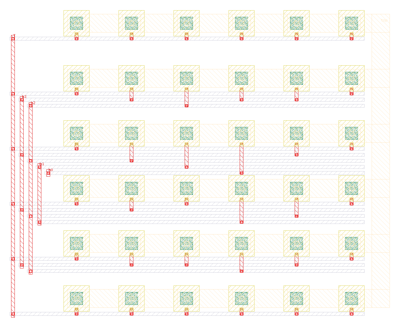
lab14_layout.py --route, drawn by KLayout with the PDK's layer colours.Your part.
- Route the common top plate in TopMetal1 and each bit’s bottom plates in the metals below, following the common-centroid map; tie the dummies to the termination net. Write the matching schematic netlist (six nets: top, bits 0–3 and termination) and rerun DRC and LVS until both are clean. Then improve on the reference solution: equalise the stub lengths so that every bit sees the same parasitic per unit.
- Extract the routed array’s parasitic capacitance (Magic’s extraction for SG13G2 is in the container) and compare the top plate’s parasitic with the 20 % that
figsrc/ch17_figs.pyassumes. - Lay out the StrongARM comparator of Lab 7 with a symmetric input pair and run DRC and LVS on it.
- Place both blocks in the JKU AMS chip template [11] and run the top-level DRC with the density rules.
Deliverable. A DRC- and LVS-clean routed capacitor array, its extracted parasitics, and a note on what changed between schematic and post-layout simulation.
All labs · Previous: Lab 13. EMG gesture recognition · Next: Lab 15. Bioimpedance IQ readout