Chapter 5Devices for Microwatt Design
A biopotential amplifier lives on a few hundred nanoamperes per transistor, so its devices sit in weak or moderate inversion, where the square law no longer applies.
- place a MOSFET in weak, moderate or strong inversion from its inversion coefficient and read its \(g_\mathrm{m}/I_\mathrm{D}\);
- explain why \(g_\mathrm{m}/I_\mathrm{D}\) peaks at about \(1/(n U_T)\) in weak inversion and what that means for noise per microampere;
- relate flicker noise to gate area and pick input-pair dimensions for a sub-100 Hz band;
- compare SG13G2 MOSFETs and SiGe HBTs as low-noise input devices (thermal noise, flicker noise, base current);
- estimate offset and gain mismatch from Pelgrom coefficients.
Which device, at what inversion level and size, gives the lowest input-referred noise for a microwatt bias current?
Part I set the targets: 1.5 µVrms of input noise from 0.5 to 100 Hz, inside a 10 µW budget per channel at 1.2 V. That budget allows about 8 µA for the whole channel, and perhaps a microampere for each input transistor. This chapter asks what an SG13G2 transistor does with so little current. Every number comes from the IHP compact models [1], simulated with ngspice in the IIC-OSIC-TOOLS container [2] by labs/spice/sg13_char.py, whose results are in figsrc/data/sg13_*.csv. The general \(g_\mathrm{m}/I_\mathrm{D}\) method is covered in Part II of The Art of Analog IC Design [4]; here it is applied to microwatt biomedical bias points.
5.1Weak, moderate and strong inversion
A MOSFET’s operating point is best described not by its overdrive voltage but by how much current it carries relative to a technology current. The inversion coefficient is
\[IC = \frac{I_\mathrm{D}}{I_\mathrm{spec}\,(W/L)}, \qquad I_\mathrm{spec} = 2n\mu C_\mathrm{ox} U_T^2,\]where \(I_\mathrm{spec}\) is the specific current of one square of channel, \(n\) the subthreshold slope factor and \(U_T = kT/q = 25.9\) mV at 300 K. Below \(IC \approx 0.1\) the device is in weak inversion: the current is carried by diffusion and grows exponentially with the gate voltage, \(I_\mathrm{D} \propto e^{V_\mathrm{GS}/(nU_T)}\). Above \(IC \approx 10\) it is in strong inversion and follows the familiar square law. Between the two is moderate inversion, where neither formula holds. One expression from the EKV model covers all three:
In weak inversion the second factor is 1, and \(g_\mathrm{m}/I_\mathrm{D}\) reaches its ceiling \(1/(nU_T)\). It falls to half of that at \(IC = 2\), and to a few per volt in strong inversion (Figure 5.1a).
The simulated \(g_\mathrm{m}/I_\mathrm{D}\) of the low-voltage devices peaks at 31.7 V⁻¹ for the NMOS and 31.9 V⁻¹ for the PMOS, so \(n = 1/(31.7 \times 0.0259) = 1.22\) and 1.21. The ratio falls to half its peak at a current density of about 1.55 µA per square for the NMOS and 0.40 µA per square for the PMOS; by the key equation that point is \(IC = 2\), so \(I_\mathrm{spec} \approx 0.78\) µA and 0.20 µA per square.
A biomedical input transistor carrying 1 µA in \(W/L = 100/10\) µm, ten squares, runs at 100 nA per square: \(IC \approx 0.13\) for the NMOS. The key equation predicts \(0.90/(nU_T) = 28.4\) V⁻¹; the simulation gives 29.6 V⁻¹, 93 % of the ceiling.
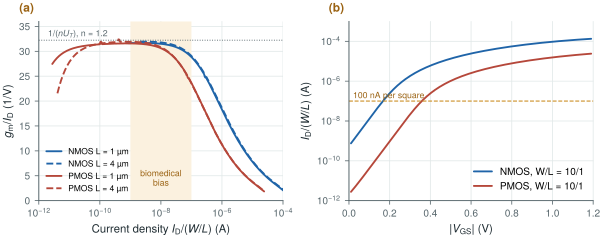
One property of these devices is worth noticing early. The low-voltage NMOS carries 100 nA per square at a gate-source voltage of only 0.17 V, and the PMOS at 0.36 V (Figure 5.1b). On a 1.2 V supply that leaves room for stacked devices and wide output swing, which is why subthreshold biasing and a 1.2 V supply go together.
5.2The gm/ID method at microwatt bias
Hand equations fail in moderate inversion, where most designs end up. The \(g_\mathrm{m}/I_\mathrm{D}\) method replaces them with lookup tables from simulation, here figsrc/data/sg13_gmid.csv, and sizes a transistor in three steps:
- choose \(g_\mathrm{m}\) from the specification, usually noise or bandwidth;
- choose \(g_\mathrm{m}/I_\mathrm{D}\), which sets the inversion level, and get \(I_\mathrm{D} = g_\mathrm{m}/(g_\mathrm{m}/I_\mathrm{D})\);
- read the current density for that \(g_\mathrm{m}/I_\mathrm{D}\) from the table and get \(W/L = I_\mathrm{D}/(I_\mathrm{D}/(W/L))\); choose \(L\) for gain, matching or flicker noise.
In a biomedical front-end the first step is almost always noise, and the thermal noise of a transistor depends on \(g_\mathrm{m}\) alone. In weak inversion the channel’s thermal noise, referred to the gate, is
\[\overline{v_n^2} = \frac{2nkT}{g_\mathrm{m}} \ \text{per hertz},\]so the noise per microampere is lowest when \(g_\mathrm{m}/I_\mathrm{D}\) is highest. That is the case for weak inversion, and why every low-power biopotential amplifier biases its input pair there [12].
The NMOS of Worked Example 5.1 has \(g_\mathrm{m} = 29.6\) µS at 1 µA. Its thermal noise is \(\sqrt{2 \times 1.22 \times 4.14\times10^{-21}/29.6\ \text{µS}} = 18.4\) nV/√Hz, which matches the simulated noise floor of 18.5 nV/√Hz. Over the 0.5–100 Hz EEG band that is \(18.4\ \text{nV} \times \sqrt{99.5} = 0.18\) µVrms per device, or 0.26 µVrms for a differential pair.
The PMOS at the same current gives 21.7 V⁻¹ and a predicted 21.5 nV/√Hz, but the simulated floor is 30.4 nV/√Hz: the models carry about twice the theoretical thermal-noise power for the PMOS. Use the simulated numbers.
Thermal noise is therefore not the problem in the EEG band. A quarter of a microvolt from a microampere-per-device pair leaves most of the 1.5 µVrms budget free. The problem is the next noise source.
The price of weak inversion is area and speed. A device at \(IC = 0.1\) needs ten times the squares of one at \(IC = 1\) for the same current, and its large gate capacitance lowers its transit frequency. For signals below a few kilohertz, speed costs nothing. Area matters, as the next section shows.
5.3Flicker noise and device area
Every MOSFET also has \(1/f\) (flicker) noise, caused by carriers trapped and released at the gate oxide interface. Referred to the gate, its density falls with frequency and with gate area:
\(K\) is a technology constant, and the corner frequency \(f_\mathrm{c}\) is where flicker noise and thermal noise are equal. Below the corner, flicker noise dominates.
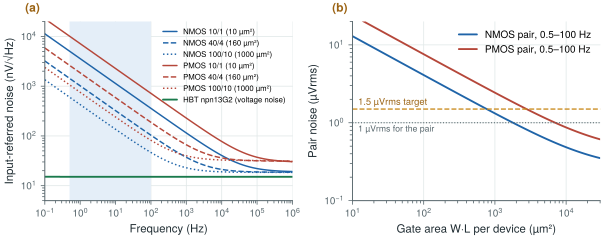
Fitting the simulated spectra gives \(K = 1.6\times10^{-10}\) V²·µm² for the NMOS and \(5.4\times10^{-10}\) V²·µm² for the PMOS: in these models the NMOS has 3.4 times less flicker-noise power. For the 100/10 µm NMOS at 1 µA, the corner is \(1.58\times10^{-13}/(18.5\ \text{nV})^2 \approx 460\) Hz, far above the EEG band.
The flicker noise of a pair integrated over the band is \(\sqrt{2K\ln(100/0.5)/(WL)}\). For the 1000 µm² NMOS, \(\sqrt{2 \times 1.58\times10^{-13} \times 5.30} = 1.29\) µVrms, nearly the whole 1.5 µVrms budget. To bring the pair to 1 µVrms including its thermal noise, each NMOS needs about 1800 µm², for example \(W/L = 134/13.4\) µm, and each PMOS about 7000 µm² (Figure 5.2b).
Two lessons follow. First, in SG13G2’s models the NMOS is the quieter device for flicker noise, the opposite of the rule of thumb that PMOS inputs are quieter. Check every new PDK rather than trusting the rule. Second, an unchopped input pair for EEG must be very large, and its gate capacitance then competes with the input capacitors of the amplifier (Chapter 8). The alternative is to move the signal above the corner frequency before it reaches the pair. That is chopping, the subject of Chapter 9, and the reason Open-BioAFE can use small input devices.
5.4MOSFET versus SiGe HBT input pairs
SG13G2 is a BiCMOS process: next to its MOSFETs it has SiGe heterojunction bipolar transistors made for radio frequencies. Their properties at a microampere look attractive for a low-noise amplifier.
- Transconductance. A bipolar transistor has \(g_\mathrm{m} = I_\mathrm{C}/U_T\) at any current, with no inversion level to choose. The npn13G2 simulates at 37.7 V⁻¹, against 29.6 V⁻¹ for the best MOSFET.
- Voltage noise. Its input-referred voltage noise is flat at 15.1 nV/√Hz at 1 µA (Figure 5.2a), with no visible flicker noise.
But a bipolar transistor draws base current, and that current flows through the electrode. The simulated current gain at 1 µA is \(\beta \approx 680\), so \(I_\mathrm{B} = 1.46\) nA. Three consequences follow:
- Current noise. The base current carries shot noise \(\sqrt{2qI_\mathrm{B}} = 21.6\) fA/√Hz, plus its own \(1/f\) part, so the shot noise alone is a lower bound. Flowing through an electrode impedance \(Z_\mathrm{e}\) it becomes a voltage noise \(i_n\lvert Z_\mathrm{e}\rvert\): 1.1 nV/√Hz for a 50 kΩ wet electrode, but 22 nV/√Hz for a 1 MΩ dry electrode and 216 nV/√Hz at 10 MΩ.
- Input resistance. \(r_\pi = \beta/g_\mathrm{m} = 680/37.7\ \text{µS} = 18\) MΩ, far below the 100 MΩ that dry electrodes need (Chapter 3).
- Offset. 1.46 nA through a 1 MΩ electrode is 1.5 mV, and any imbalance between the two electrodes turns it into a differential offset that drifts with the electrodes.
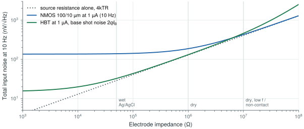
Figure 5.3 puts the trade-off on one axis. With wet electrodes and no chopping, the HBT is the quieter input device by almost a factor of ten at 10 Hz. Above about 6 MΩ of electrode impedance, its base current makes it noisier. It also loads the electrode with 18 MΩ and needs a DC path for its base current, which a capacitively coupled input does not provide. Open-BioAFE must support dry electrodes and uses a capacitively coupled, chopped input (Chapter 7, Chapter 9), so its input pair is MOS. The HBTs still earn their place in the bandgap reference and in bias circuits.
Gate leakage. At 130 nm the thin gate oxide conducts. A 250/4 µm thin-oxide NMOS biased like an input device leaks 3–25 pA through its gate in the SG13G2 models, depending on its gate–drain voltage; a thick-oxide device of the same size leaks about 10⁻²⁰ A. A few picoamperes are harmless in most circuits, but not on a node biased through a teraohm pseudo-resistor (Chapter 8, Section 8.5). The thick-oxide device pays with about 2.7 times the flicker-noise power of the thin-oxide one at the same area.
5.5Matching
Two transistors drawn identically are never identical. Random variations in dopant number, oxide charge and edge roughness give each device a slightly different threshold voltage and current factor. Pelgrom’s law [9] says the spread of the difference between two devices falls with the square root of their area:
The SG13G2 mismatch models state the coefficients directly (in sg13g2_moslv_mismatch.lib): \(A_{V_T} = 3.9\) mV·µm and \(A_\beta = 0.5\) %·µm for the low-voltage NMOS, 2.2 mV·µm and 0.33 %·µm for the PMOS. MIM capacitors match to 1 %·µm (cap_carea_mm in the capacitor library), and the HBT saturation current to 3.8 % for a single minimum device.
Input pair. Two 1800 µm² NMOS devices (Worked Example 5.3) have \(\sigma(\Delta V_\mathrm{T}) = 3.9/\sqrt{1800} = 0.092\) mV. Three standard deviations, 0.28 mV, is about 190 times the 1.5 µVrms noise target. No reasonable area brings offset down to the noise level; it has to be removed by chopping (Chapter 9) or by a DC servo loop (Chapter 10).
Bias mirror. In weak inversion a threshold mismatch turns into a current mismatch multiplied by \(g_\mathrm{m}/I_\mathrm{D}\): \(\sigma(\Delta I/I) \approx \sigma(\Delta V_\mathrm{T})\,g_\mathrm{m}/I_\mathrm{D}\). A 10 µm² PMOS mirror at \(g_\mathrm{m}/I_\mathrm{D} = 30\) V⁻¹ gives \((2.2/\sqrt{10}\ \text{mV}) \times 30 = 2.1\,\%\). The same mirror biased in strong inversion at 5 V⁻¹ gives 0.35 %. Bias current mirrors should therefore run in strong inversion, the opposite of the input pair.
Capacitors. The 12-bit SAR of Chapter 14 needs unit capacitors matched to 0.26 %. At 1 %·µm that takes \((1/0.26)^2 \approx 15\) µm² per unit, a figure Chapter 17 uses.
Bias the input pair in weak inversion (\(g_\mathrm{m}/I_\mathrm{D} \approx 30\) V⁻¹), where each microampere buys the least thermal noise; at 1 µA per device thermal noise uses only a sixth of the EEG budget. Use NMOS inputs in SG13G2, whose flicker noise is lower in the models. Flicker noise and offset then dominate, and neither is cheap to fix with area: an unchopped pair needs about 1800 µm² per device and still has 0.3 mV of offset. Chopping fixes both at once, so the input pair can stay small. Bias mirrors go the other way, into strong inversion, for matching.
Input pair: SG13G2 low-voltage NMOS in weak inversion, about 1 µA per device, \(g_\mathrm{m}/I_\mathrm{D} \approx 30\) V⁻¹ (thermal noise 18.5 nV/√Hz per device). Size set by chopping (Chapter 9), not by flicker noise. HBTs for the reference and bias only.
Do not size a biomedical amplifier with square-law equations. At 100 nA per square the device is in weak inversion, \(g_\mathrm{m} = 2I_\mathrm{D}/V_\mathrm{ov}\) is meaningless, and the overdrive voltage is negative. Read \(g_\mathrm{m}/I_\mathrm{D}\), noise and current density from simulated tables of your own PDK, as in this chapter, and check rules of thumb such as “PMOS is quieter” against them.
Lab 3 characterises \(g_\mathrm{m}/I_\mathrm{D}\), flicker noise versus \(W\!\cdot\!L\) and HBT versus MOS input noise in SG13G2; its lookup tables are reused in Labs 4 and 5. Start from labs/spice/sg13_char.py, which runs every simulation of this chapter in the IIC-OSIC-TOOLS container, and add the corners and lengths you need.
Read with this chapter. Sarpeshkar [12] (subthreshold design, noise–power limits), Razavi [13] (device noise), Pelgrom [9] (matching), The Art of Analog IC Design [4] (Part II: the transistor and \(g_\mathrm{m}/I_\mathrm{D}\)), the IHP-Open-PDK documentation [1].
- The inversion coefficient places a MOSFET on one curve from weak to strong inversion; SG13G2’s low-voltage devices have \(n \approx 1.2\) and a \(g_\mathrm{m}/I_\mathrm{D}\) ceiling of about 32 V⁻¹.
- In weak inversion thermal noise per microampere is lowest: 18.5 nV/√Hz for a 1 µA NMOS, 0.26 µVrms for a pair over 0.5–100 Hz.
- Flicker noise dominates the EEG band: an unchopped NMOS pair needs about 1800 µm² per device for 1 µVrms; in these models the NMOS is quieter than the PMOS.
- The SiGe HBT has more \(g_\mathrm{m}\) and no voltage flicker noise, but its 1.5 nA base current adds noise, loads the electrode (18 MΩ) and makes offset; it suits wet electrodes, not dry ones.
- Pelgrom coefficients: 3.9 mV·µm (NMOS), 2.2 mV·µm (PMOS), MIM 1 %·µm. Input offset needs chopping or a servo loop; mirrors belong in strong inversion.