Chapter 20ΔΣ Circuits: Discrete-Time, Continuous-Time and Incremental
From the loop filter on paper to integrators in silicon, and to the incremental converter that serves the high-resolution Open-BioAFE channels.
- build switched-capacitor integrators and set their OTA requirements;
- design continuous-time loops with resistive or Gm-C integrators and use their inherent anti-aliasing;
- handle excess loop delay;
- design an incremental ΔΣ converter for multiplexed channels;
- design and budget the decimation filter (CIC/sinc\(^K\) and half-band FIR).
How do you implement the 2nd-order incremental modulator of Open-BioAFE and its decimator within the power budget?
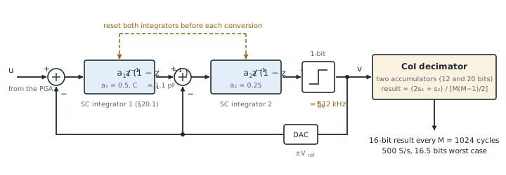
Chapter 19 settled the theory: a second-order incremental modulator with a 1-bit quantiser, 1024 cycles per conversion and a 512 kHz clock gives 16.5 bits. This chapter builds it, with the converter range of ±0.5 V differential used throughout Part III, and checks it against the 1–3 µW per channel that Chapter 14 estimated. Figure 20.1 shows the converter as it is built here.
20.1Switched-capacitor integrators
A discrete-time loop builds each integrator from an OTA, an integrating capacitor \(C_\mathrm{int}\) and a sampling capacitor \(C_\mathrm{s}\) switched at the clock rate. Each period, \(C_\mathrm{s}\) samples the input minus the DAC’s feedback and dumps its charge into \(C_\mathrm{int}\), so the integrator gain is \(C_\mathrm{s}/C_\mathrm{int}\): a capacitor ratio, accurate to a fraction of a percent and independent of the clock frequency (Figure 20.2).
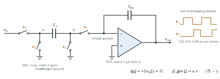
The first condition is \(kT/C\) noise averaged over a conversion. The incremental decimator weights the \(M\) samples of the first integrator by a ramp, which averages their noise by an effective factor of \(3M/4\); counting both sides and both clock phases gives about \(4kT/C_\mathrm{s}\) per sample. The second condition asks the OTA to settle by \(n_\tau\) time constants in half a clock period, with feedback factor \(\beta\).
Capacitor. 16 bits over 1 V is an LSB of 15.3 µV; its quantisation-equivalent noise is \(15.3/\sqrt{12} = 4.4\) µV. With \(M = 1024\), \(C_\mathrm{s} \ge 1.1\) pF, matching the 1.2 pF that Chapter 14 found for an OSR of 128.
OTA. A half clock period is 0.98 µs. With a 1-bit DAC, incomplete but linear settling only scales the integrator gain, which the loop tolerates, so settling to 1 % (five time constants) is enough rather than to 16 bits. With \(\beta \approx 0.67\) that needs a GBW of 1.2 MHz; on 2.5 pF of load it is 19 µS, about 1 µA at \(g_\mathrm{m}/I_\mathrm{D} = 20\) V⁻¹. The second integrator’s errors are shaped by the first, so it can run on half that.
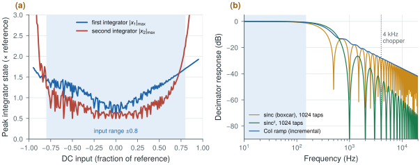
The integrators must also swing. Simulating the loop (figsrc/ch20_figs.py) with \(a_1 = a_2 = 0.5\) over inputs of ±0.8 of the reference, the first integrator peaks at 1.7 times the reference and the second at 2.25 times (Figure 20.3a). At 1.2 V a fully differential OTA swings about ±0.9 V differential, so with a 0.5 V reference the second integrator would overload. Halving \(a_2\) (and adjusting the decimator’s weights to match) halves its swing.
20.2Continuous-time ΔΣ
A continuous-time loop integrates the input directly, with RC or Gm-C integrators, and samples only at the quantiser. Two advantages follow. The loop filter in front of the sampler is an inherent anti-alias filter, attenuating whatever would fold back from near the clock frequency. And there are no sampling switches at the input, so no \(kT/C\) at the input and no charge kickback into the electrodes’ side.
The costs are equally real. The integrator gains are now \(1/(RC)\) or \(g_\mathrm{m}/C\), absolute values that vary by ±20 % or more over process and temperature, so the noise transfer function moves and must be trimmed. The feedback DAC’s pulses must be clean in time, because clock jitter shifts their edges and injects noise directly at the input (Chapter 13). And resetting a continuous-time loop between conversions, as an incremental converter must, is awkward. For a multiplexed, incremental biosignal converter, discrete-time switched-capacitor integrators are the better fit. Continuous-time loops shine in free-running, wideband converters.
20.3Excess loop delay
In a continuous-time loop the quantiser and DAC cannot respond instantly. The delay between the sampling instant and the DAC pulse, the excess loop delay, adds phase lag to the loop and, uncorrected, raises the in-band noise or makes a high-order loop unstable. The standard fix is a direct feedback path from the quantiser’s output to its input that compensates the delay, together with a half-period delay budget. A discrete-time loop has no such problem: its timing is defined by the clock phases, and the quantiser has a whole phase to decide.
20.4Incremental ΔΣ
The incremental converter resets both integrators at the start of each conversion, runs 1024 cycles, and resets again. Reset is easy in a switched-capacitor integrator: a switch across each \(C_\mathrm{int}\) discharges it during the first phase. Because each conversion starts from zero, the converter can serve one channel for 1024 cycles and then switch to another without memory. Open-BioAFE nevertheless gives each channel its own modulator. Multiplexing eight channels would need an 8 × 512 kHz = 4 MHz clock, and four times the OTA bandwidth and current, for no saving in total energy.
The decimator for a second-order incremental converter is a cascade of two integrators (CoI): an accumulator of the output bits, and an accumulator of that accumulator, whose final values combine into the estimate of Chapter 19. It needs about \(\log_2(M(M-1)/2) = 19\) bits of word length, two adders and two registers per channel, a few hundred gates clocked at 512 kHz.
The demo below converts 8001 DC inputs with the loop of Chapter 19 and plots the error of each. Compare a first-order loop read by a counter with the second-order loop and its cascade-of-integrators filter as M grows.
20.5Decimation
The decimator is a digital filter, and its frequency response matters (Figure 20.3b). A free-running modulator usually uses a sinc\(^K\) (CIC) filter, a cascade of \(K\) moving averages, followed by half-band FIR stages. A moving average over a conversion has exact notches at every multiple of the output rate. The incremental CoI filter weights the samples by a ramp instead, and has no exact notches: its response falls as about \(1/(\pi k)\) at the \(k\)-th multiple of the output rate. At 4 kHz, the eighth multiple of 500 S/s, it gives −28 dB. It droops by 0.9 dB at 150 Hz, the top of the ECG band, which a small digital equaliser can correct.
The chopper’s ripple at 4 kHz is the one in-band-adjacent tone the decimator must handle. Because the chopper clock is locked to the conversion rate, the ripple aliases exactly to DC, where it adds to the offset and the high-pass removes it; the decimator’s 28 dB of attenuation reduces it further. A longer, smoother decimator (a sinc² over the same window, for example) adds attenuation at the cost of resolution per cycle.
figsrc/ch20_figs.py.20.6The reference design
Table 20.1. The Open-BioAFE ECG/EEG converter, per channel.
| Block | Design | Current or energy |
|---|---|---|
| Integrator 1 | SC, \(C_\mathrm{s} = 1.1\) pF, \(a_1 = 0.5\), chopped OTA, settles to 1 % | about 1 µA |
| Integrator 2 | SC, \(a_2 = 0.25\) (scaled for swing) | about 0.5 µA |
| Quantiser | dynamic comparator, 1 decision per cycle | about 50 fJ × 512 k = 26 nW |
| DAC | 1-bit, switched reference | inherently linear |
| Decimator | CoI, 19-bit, 512 kHz | tens of nanowatts |
| Total | 1024 cycles, 500 S/s, 16.5 bits worst case | about 1.9 µW at 1.2 V |
The first integrator’s OTA is itself chopped, so that its offset and flicker noise do not limit the converter, and its chopper runs from the same clock as the front-end’s.
Use switched-capacitor integrators: their gains are capacitor ratios, they reset easily for incremental operation, and their timing is defined by the clock. Size the first sampling capacitor from \(kT/C\) averaged over the conversion, about 1.1 pF, and let the OTA settle only to 1 %, because a 1-bit loop tolerates linear gain error. Scale the second integrator for swing. Give each channel its own modulator. Expect about 1.9 µW per channel, within the estimate of Chapter 14, and remember that the CoI decimator has no notches: the synchronous chopper clock, not the filter, is what neutralises the ripple.
Per channel: second-order discrete-time incremental ΔΣ, 1-bit, 512 kHz, \(M = 1024\), \(a_1 = 0.5\), \(a_2 = 0.25\), \(C_\mathrm{s1} = 1.1\) pF, chopped first OTA of about 1 µA, CoI decimator with a droop equaliser; about 1.9 µW at 1.2 V for 16.5 bits at 500 S/s.
Assuming the decimator removes every tone at a multiple of the output rate. Only a moving-average (sinc) decimator has exact notches there; the incremental cascade-of-integrators filter attenuates them by only \(1/(\pi k)\). Check the filter you actually built at the chopper frequency and at the mains harmonics.
Lab 10 builds the Lab 9 loop with switched-capacitor integrators and a 1-bit quantiser and compares it with the ideal model. Start by rerunning figsrc/ch20_figs.py with \(a_2 = 0.25\) and the matching CoI weights, and check that the swing halves and the resolution holds.
Read with this chapter. Schreier, Temes and Pavan [10] (switched-capacitor and continuous-time loops, incremental converters, decimation), python-deltasigma [27].
- Switched-capacitor integrators set their gains by capacitor ratios and reset easily, which suits an incremental converter.
- The first sampling capacitor needs about 1.1 pF for 16 bits with 1024 cycles; the OTA needs to settle only to 1 %, about 1 µA.
- Within ±0.8 of the reference the second integrator swings to 2.25 times the reference, so it is scaled down.
- Continuous-time loops give inherent anti-aliasing but absolute coefficients, jitter sensitivity and awkward reset.
- The CoI decimator has no notches: −28 dB at the 4 kHz chopper frequency and 0.9 dB of droop at 150 Hz.
- The per-channel converter costs about 1.9 µW.