Chapter 10Input Impedance, DC Servo Loops and Offset Rejection
Electrodes bring hundreds of millivolts of DC and megaohms of source impedance. The front-end must reject the first without loading the second.
- derive the input impedance of a capacitively coupled, chopped front-end;
- design a positive-feedback impedance-boosting loop;
- design a DC servo loop (DSL) that rejects ±300 mV of electrode offset;
- compare DC-coupled and AC-coupled front-ends;
- state the trade-offs for dry electrodes.
How do you tolerate ±300 mV of electrode offset and keep the input impedance high enough for dry electrodes?
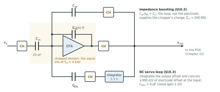
Chapter 9 chopped the capacitively coupled IA and paid for it twice. Its input impedance fell to 6.25 MΩ, and something less obvious happened too: the input chopper sits in front of the input capacitors, so it turns the electrode’s DC offset into a square wave at the chopping frequency, which the capacitors pass. The chopped CCIA no longer blocks the offset. This chapter restores both properties, with an impedance-boosting loop and a DC servo loop (Figure 10.1).
10.1Input impedance of chopped CCIAs
An unchopped CCIA loads each electrode with its input capacitor: 20 pF is 160 MΩ at 50 Hz and rises at lower frequencies. Chopping replaces this with a switched-capacitor resistor. On every chopper transition the voltage across each input capacitor reverses, and the electrode supplies the charge, twice per period:
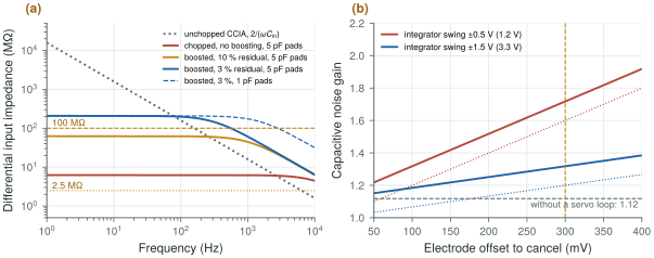
The chopped impedance is flat with frequency up to the chopping frequency, so at low frequencies it is far lower than the unchopped one (Figure 10.2a). With \(C_\mathrm{in} = 20\) pF at 4 kHz it is 6.25 MΩ. That passes the 2.5 MΩ the ECG standards require, but a 1 MΩ dry electrode in front of it loses 14 % of the signal, and an imbalance between two dry electrodes turns common mode into differential mode through the divider (Chapter 4).
The pads add a second, frequency-dependent load. Bond pad, ESD protection and wiring add a few picofarads to ground at each input: 5 pF is 640 MΩ at 50 Hz and 32 MΩ at 1 kHz. That caps whatever the amplifier achieves, and it is also part of the common-mode input impedance of Chapter 4.
10.2Positive-feedback impedance boosting
The charge that the chopped input capacitors draw from the electrode can be supplied from inside the amplifier instead. A positive-feedback loop takes the amplifier output, which carries the amplified input, chops it with the same clock, and drives it through a small capacitor \(C_\mathrm{pf}\) back onto the input nodes. Chosen so that \(C_\mathrm{pf}A_\mathrm{M} \approx C_\mathrm{in}\), it pre-charges the input capacitors at each transition, and the electrode supplies only what the loop does not.
If the loop supplies all but a fraction \(\varepsilon\) of the charge, the impedance rises by \(1/\varepsilon\):
\[Z_\mathrm{boost} \approx \frac{1}{2 f_\mathrm{ch} C_\mathrm{in}\,\varepsilon}.\]\(\varepsilon\) is set by the matching of \(C_\mathrm{pf}A_\mathrm{M}\) to \(C_\mathrm{in}\) and by the gain accuracy. Pushing it too far risks instability, because the loop is positive feedback: an overcompensated loop has a negative input resistance.
From 6.25 MΩ to the 100 MΩ target is a factor of 16, so the loop must leave less than 6 % of the charge to the electrode. With a 10 % residual the impedance is 62 MΩ; with 3 %, 208 MΩ at 10 Hz.
The pads then take over at higher frequencies. With 5 pF per input, the 3 % design falls to 61 MΩ at 1 kHz; with 1 pF it stays near 200 MΩ to a few hundred hertz (Figure 10.2a). Keeping the input pads small, and guarding them with a driven shield (Chapter 12), is part of the input-impedance design.
10.3The DC servo loop
The electrode offset must be stopped before the LNA’s gain of 100 turns ±300 mV into ±30 V. In the chopped CCIA the input capacitors cannot do it, because the input chopper has already turned the offset into a ±300 mV square wave. A DC servo loop removes it. An integrator watches the LNA’s output after the output chopper, where the offset is DC, and slowly accumulates it. Its output, chopped by the same clock, drives a capacitor \(C_\mathrm{DSL}\) onto the input nodes, injecting a charge that cancels the offset’s charge through \(C_\mathrm{in}\).
The loop has two design constraints. To cancel an offset \(V_\mathrm{off}\) with an integrator that can swing \(\pm V_\mathrm{DSL}\):
The loop also sets the amplifier’s high-pass corner, now through an integrator with a well-defined time constant \(\tau_\mathrm{int}\) rather than through a pseudo-resistor’s uncertain one (Chapter 8). The pseudo-resistors then only bias the OTA’s input nodes, and because the signal there sits at the chopping frequency they can be as small as about 10 GΩ, far above the 200 MΩ of \(C_\mathrm{fb}\) at 4 kHz. That matters in SG13G2: the thin-oxide input devices leak picoamperes through their gates, which a 10 GΩ bias turns into tens of millivolts but a teraohm pseudo-resistor cannot carry (Chapter 8, Section 8.5).
The price is noise. \(C_\mathrm{DSL}\) hangs on the OTA’s input nodes, and it adds to the capacitive noise gain \((C_\mathrm{in} + C_\mathrm{fb} + C_\mathrm{gate} + C_\mathrm{DSL})/C_\mathrm{in}\). The integrator’s own noise also reaches the input, attenuated by \(C_\mathrm{DSL}/C_\mathrm{in}\).
With a 1.2 V integrator swinging ±0.5 V around mid-supply, \(C_\mathrm{DSL} \ge 0.3/0.5 \times 20\ \text{pF} = 12\) pF. The noise gain rises from 1.12 to 1.72, which raises the 0.27 µVrms chopped input noise of Chapter 9 by 54 %.
With an integrator built from the 3.3 V thick-oxide devices, swinging ±1.5 V, \(C_\mathrm{DSL} = 4\) pF and the noise gain is 1.32, 18 % above the case without a loop (Figure 10.2b). Its current is tiny, because the loop works at DC, so the higher supply costs well under a microwatt.
The high-pass corner: with \(C_\mathrm{DSL}/C_\mathrm{fb} = 4\ \text{pF}/200\ \text{fF} = 20\), a 0.5 Hz corner needs \(\tau_\mathrm{int} = 20/(2\pi \times 0.5) = 6.4\) s. An active-RC integrator with 1 pF and a thick-oxide pseudo-resistor (about \(10^{13}\) Ω at body temperature) gives about 10 s. A small integrating current from a subthreshold transconductor does the same.
figsrc/ch10_figs.py.10.4DC-coupled versus AC-coupled front-ends
A front-end can treat the electrode offset in two ways. DC coupling keeps it and digitises it along with the signal. The offset carries information: when an electrode moves or loses contact, its offset jumps, so a DC-coupled channel can flag motion artefacts and lead-off directly. The cost is dynamic range. Chapter 2 found that a DC-coupled chain needs about 103 dB, almost 17 bits, and no gain can be applied before the converter.
AC coupling removes the offset in the analog domain and digitises only the signal, so gain can be applied early and the converter needs less range. Open-BioAFE is AC-coupled through its DC servo loop, but it keeps the information. The servo integrator’s output is a measure of the electrode offset, and the SAR converter can sample it a few times per second. The channel thus reports both the clean biosignal and the slowly varying electrode potential that marks artefacts and contact problems, without spending converter range on it. The impedance-tracking channel of Chapter 28 adds the electrode impedance to that picture.
10.5Dry electrodes
Dry electrodes concentrate every problem of this chapter: source impedance of 1 MΩ or more at low frequency, larger and faster-changing offsets, and more motion artefacts (Chapter 3). Each front-end option buys something and costs something:
- Impedance boosting brings the chopped CCIA above 100 MΩ, at the price of a positive-feedback loop that must be trimmed and kept stable, plus small, guarded input pads.
- A larger servo range handles larger offsets, at the price of a larger \(C_\mathrm{DSL}\) and more noise, or of a 3.3 V integrator.
- A lower chopping frequency raises the input impedance directly (Chapter 9), at the price of larger input devices to keep the flicker corner below it.
- Active electrodes, which buffer the signal at the skin (Chapter 12), remove the cable and pad loading entirely, at the price of electronics in every electrode.
Open-BioAFE combines the first two on chip and leaves active electrodes as a system option.
A chopped CCIA no longer blocks DC, so it needs a DC servo loop, and its input impedance falls to \(1/(2f_\mathrm{ch}C_\mathrm{in})\), so dry electrodes need boosting. Size the servo capacitor from the offset and the integrator’s swing: a 3.3 V integrator cuts it from 12 to 4 pF and the noise penalty from 54 % to 18 %. Let the servo loop, not a pseudo-resistor, define the high-pass corner. Boost the impedance by at least 16 and keep the input pads to a picofarad or two, or the pads set the limit. And read the servo integrator: it tells you the electrode offset for free.
DC servo loop with a 3.3 V thick-oxide integrator (±1.5 V), \(C_\mathrm{DSL} = 4\) pF, ±300 mV offset range, high-pass corner 0.5 Hz (selectable down to 0.05 Hz), integrator output sampled by the SAR as an electrode-offset monitor. Positive-feedback boosting to above 100 MΩ at 10 Hz (residual ≤ 6 %), input pads below 2 pF each. Total LNA noise gain about 1.32: chopped input noise about 0.36 µVrms over 0.5–100 Hz.
Measuring input impedance with an AC analysis. The chopped input’s impedance is a switched-capacitor effect that a small-signal .ac run does not see; it reports the unchopped \(2/(j\omega C_\mathrm{in})\), hundreds of times too high at low frequencies. Measure it in a transient or periodic steady-state simulation: drive the input through a large resistor and compare the signal on both sides, or average the input current over many chopping periods.
Lab 5 measures the input impedance with and without a chopper and verifies ±300 mV offset tolerance with the DC servo loop. Use figsrc/ch10_figs.py to predict the impedance and the noise gain before you simulate, then compare.
Read with this chapter. Yazicioglu, Van Hoof and Puers [8], Spinelli et al. [18], Chi et al. [19].
- Chopping makes the CCIA’s input impedance \(1/(2f_\mathrm{ch}C_\mathrm{in})\), 6.25 MΩ at 4 kHz with 20 pF, flat with frequency; the pads’ capacitance adds a frequency-dependent limit.
- Positive-feedback boosting raises it by \(1/\varepsilon\); dry electrodes need \(\varepsilon\) below about 6 %.
- The input chopper defeats the CCIA’s DC blocking, so a DC servo loop must cancel the electrode offset: \(C_\mathrm{DSL} \ge (V_\mathrm{off}/V_\mathrm{DSL})C_\mathrm{in}\).
- The servo capacitor raises the noise gain: 1.72 with a 1.2 V integrator, 1.32 with a 3.3 V one.
- The servo integrator’s output reports the electrode offset, keeping the information of a DC-coupled channel without its dynamic range.