Chapter 14The Open-SERDES Architecture
Every decision of the last thirteen chapters on a few pages: what the project delivers, the blocks and clocks, the number each block must meet at 5 and at 10 Gb/s, the test chip around them, and the plan to get there.
In this chapter you will learn
Say what the project delivers, and which chapter feeds each deliverable.
Read the complete Open-SERDES block diagram and follow a bit from the 16-bit TX word to the 16-bit RX word.
Trace every clock in the chip from the 50 MHz reference to the last divider, with its frequency and phase.
Use the block specification table to find the 5 and 10 Gb/s targets, and the chapter that derives them, for any block you design.
Explain why the same architecture reaches 10 Gb/s, and list the six things that must change.
Build a first-cut power budget from tail currents and convert it to energy per bit.
Place the transceiver on a test chip: its test logic, its floorplan and its package.
Defend the ten main architecture decisions, and map the five project phases to what each must prove.
14.1What Open-SERDES delivers
Before the block diagram, the goal. Open-SERDES is not only a chip: it is a chip, the flow that produced it and the data that proves it, all in one public repository. The project’s own summary has five highlights:
Project highlights
The first open multi-Gb/s mixed-signal SerDes on an open PDK.
A 10 Gb/s-capable NRZ transceiver, with TX, RX, PLL and CDR, in SG13G2, guaranteed at 5 Gb/s (Section 14.4).
One reproducible flow from the channel model to GDS (Chapter 15).
A link model calibrated against post-layout simulation and, later, silicon (Section 15.2).
Everything public: design files, models and lab data.
Table 14.1 turns the highlights into six things anyone will be able to download, and points to the chapters that produce the numbers inside each one.
| Deliverable | What it is | Phase | Built in |
|---|---|---|---|
| GDSII | the tape-out-ready 5/10 Gb/s transceiver test chip of Section 14.5 | 2 | Chapters 9, 10, 12, 13 and 15 |
| RTL + testbenches | serializer, deserializer, PRBS generator and checker, CDR loop logic, and their benches | 1–2 | Sections 9.2, 10.6, 13.6 and 15.3 |
| Link model | the Python link simulator, statistical eye and GUI, driven by one spec file | 0 | Chapters 4 and 16 |
| Cell library | reusable HBT/CML drivers, latches, muxes and CTLE cells for SG13G2 | 1 | Chapters 7, 9 and 10 |
| Documentation | the GitHub repository and this tutorial | all | every chapter |
| Paper + data | a journal or conference paper (IEEE JSSC or TCAS, SMACD 2027) with open measurement data | 3 | Section 15.5 |
The test of success
Clone the repository, run make all, and reproduce the chip, the models and the measurements. Every design choice in this chapter should make that sentence easier to keep, not harder.
14.2The complete transceiver
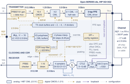
Figure 14.1 puts the whole chip on one page. It is a single-lane transceiver: one transmitter, one receiver and one clock generator on the same SG13G2 die, connected to each other through the off-chip REF channel (Section 3.7) or through an on-chip loopback.
Transmit path
A 16-bit word arrives every 3.2 ns (312.5 MHz), from the user or from the on-chip PRBS7/31 generator (Section 2.2). CMOS on 1.2 V performs the first 16:4 serialization; HBT CML on the 2.5 V analog supply performs the 4:2 and the final half-rate 2:1, built three times so the driver receives \(D_{n+1}\), \(D_n\) and \(D_{n-1}\) for its three FFE taps (Sections 9.2 and 9.5). The CML driver launches 1 Vppd into 50 Ω per side (Section 9.4).
Receive path
Behind the ESD diodes and the 100 Ω termination (Section 9.6), a loopback multiplexer selects the pad or the near-end loopback. The CTLE adds 0–12 dB of peaking (Chapter 7), the DFE summer subtracts \(w_1\) and \(w_2\) times the previous decisions (Section 8.2), and four samplers decide: data D0, D1 and edges E0, E1 (Section 10.2). The deserializer delivers 16 data and 16 edge bits at 312.5 MHz (Section 10.6); the PRBS checker counts errors.
Clocking and control
An integer-N PLL with an LC VCO multiplies the 50 MHz reference by \(N=50\) to 2.5 GHz (Chapter 12). The TX gets it through buffers and \(\div2\) dividers; the RX gets I and Q from a polyphase filter (Section 12.5), rotated by two phase interpolators (PIs) under the digital CDR loop filter (Section 13.6). An SPI port writes every setting.
14.2.1The clocking plan
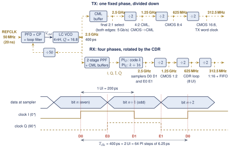
Figure 14.2 follows each clock from the reference to the last flip-flop. All of the frequencies come from one relation between the bit rate, the half-rate clock and the word rate.
Key equation · The Open-SERDES clock frequencies
\[f_\mathrm{clk} = \frac{f_\mathrm{b}}{2} = N f_\mathrm{ref} = 2.5\,\mathrm{GHz},\qquad f_\mathrm{word} = \frac{f_\mathrm{b}}{16} = 312.5\,\mathrm{MHz},\qquad \Delta t_\mathrm{PI} = \frac{1}{64\,f_\mathrm{clk}} = 6.25\,\mathrm{ps} \tag{14.1}\]
The TX needs one clock phase: the final 2:1 mux uses both edges of the 2.5 GHz clock as its select (Section 9.2). The RX needs four phases half a UI apart: data samplers on the edges of I (eye centers), edge samplers on the edges of Q (crossings), all moved together by the CDR in 6.25 ps steps. The RX dividers run from the recovered clock, so the deserializer and the CDR logic sit in a clock domain that is not phase-locked to the TX word clock; a small FIFO crosses back to the core (Section 10.6). In near-end loopback both ends share the PLL, so the frequency offset is zero. Through a board to a second chip, the CDR must absorb up to \(\pm300\) ppm (Section 13.6). Section 14.4 keeps this plan for a 10 Gb/s target with the clocks doubled, and takes I and Q from a \(\div2\) instead of the polyphase filter.
What this means for your design
Three boundaries organize the chip, and most integration bugs live on them: the speed boundary between CMOS and CML (1.25 Gb/s in the TX, 2.5 Gb/s in the RX), which needs level converters and half a slow-clock cycle of timing margin; the supply boundary between 1.2 and 2.5 V, where every \(V_\mathrm{CE}\) must stay below \(\mathrm{BV}_\mathrm{CEO}\); and the clock-domain boundary between the TX clock and the recovered RX clock. Draw all three on the floorplan first.
14.3Block specifications
Table 14.2 is the contract between the system model and the circuit designers: one row per block, the numbers that block must meet, and the chapter where each number is derived. It has two target columns. The 5 Gb/s column is the baseline that the rest of this book derives, and the pass criterion of first silicon. The 10 Gb/s column is the design target of Section 14.4: every high-speed block is sized for it, and “same” means the 5 Gb/s value already covers it. Values marked \(^\dagger\) are first estimates from hand analysis or behavioral models. They must be confirmed by simulation in SG13G2, and some of them will move.
| Block | Key specification | 5 Gb/s: guaranteed | 10 Gb/s: target | Derived in |
|---|---|---|---|---|
| Link | rate, BER, channel | 5 Gb/s NRZ; BER \(\le10^{-12}\) over REF (\(-17.4\) dB at 2.5 GHz); margin up to 20 dB | 10 Gb/s NRZ; BER \(\le10^{-12}\) over REF-10 (\(-15.3\) dB at 5 GHz) | Sections 1.4, 3.7 and 14.4 |
| Serializer | ratio, clocks, jitter | 16:1 from 16 b at 312.5 MHz; CMOS 16:4, CML 4:2, half-rate CML 2:1; DCD + DDJ \(\le8\) ps\(^\dagger\) | 16 b at 625 MHz; CMOS 16:8, CML 8:4, 4:2, half-rate 2:1; DCD + DDJ \(\le4\) ps\(^\dagger\) | Section 9.2 |
| TX driver | topology, swing | HBT CML, 50 Ω back-termination per side; 0.8–1.0 Vppd (\(I_T\) = 16–20 mA); every \(V_\mathrm{CE}<\mathrm{BV}_\mathrm{CEO}\approx1.6\) V at all corners | same; 20–80 % edges \(\le30\) ps\(^\dagger\) | Section 9.4 |
| TX FFE | taps, range, resolution | \(c_{-1}, c_0, c_1\) with \(\sum\lvert c_k\rvert=1\); \(c_1\) to \(-0.25\) (6 dB), \(c_{-1}\) to \(-0.1\); 5-bit current cells (steps of 1/32) | same | Sections 6.2 and 9.5 |
| Termination, pad | impedance, \(C_p\), return loss | 100 Ω diff., \(\pm10\) % after 3–4-bit trim; \(C_p\le0.85\) pF (0.63 pF estimated\(^\dagger\)); RL \(\ge10\) dB at \(f_\mathrm{N}\) | RL \(\ge10\) dB at 5 GHz: \(C_p\le0.42\) pF, so the T-coil is required | Sections 9.3 and 9.6 |
| CTLE | peaking, poles, noise | 0–12 dB programmable; \(f_{p1}\approx2.5\) GHz, \(f_{p2}\ge7.5\) GHz; noise \(\le0.25\) mV rms\(^\dagger\) | same peaking; \(f_{p1}\approx5\) GHz, \(f_{p2}\ge15\) GHz | Chapter 7 |
| DFE | taps, loop timing | half-rate, 2 taps, direct feedback; \(w_1\) up to \(0.5\,p_0\), \(w_2\) to \(\pm0.15\,p_0\); tap-1 loop \(\approx\)140 ps\(^\dagger\) \(<\) 1 UI; loop unrolling as fallback | tap 1 unrolled (the \(\approx\)140 ps loop exceeds the 100 ps UI); tap 2 direct | Section 8.2 |
| Samplers | count, sensitivity, offset | 4 HBT CML master–slave (D0 E0 D1 E1); \(V_\mathrm{sens}\approx20\) mV; offset \(\sigma\approx4.9\) mV raw\(^\dagger\), \(\pm0.46\) mV after 5-bit trim; \(\tau\le5\) ps; aperture \(\le0.2\) UI | 6 (two per data phase for the unrolled tap, E0, E1); \(\tau\le3\) ps\(^\dagger\); aperture \(\le20\) ps | Sections 10.2 and 10.4 |
| Deserializer | ratio, output | 1:16 CMOS; 16 data + 16 edge bits at 312.5 MHz; two extra latches on the edge path; FIFO to the core | one CML 1:2 first, then CMOS to 16 + 16 bits at 625 MHz | Sections 10.6 and 10.3 |
| PLL | architecture, jitter | integer-N CP-PLL, \(f_\mathrm{ref}\) = 50 MHz, \(N\) = 50; LC VCO 2.5 GHz (4 nH, \(Q\) = 16.8); \(K_\mathrm{VCO}\approx2\pi\times150\) MHz/V; \(f_u\approx3\) MHz; RJ \(\le1.0\) ps rms\(^\dagger\) | LC VCO at 10 GHz, \(N\) = 200; RJ \(\le0.5\) ps rms\(^\dagger\) | Chapter 12 |
| Quadrature | accuracy | 2-stage polyphase + CML buffers; I/Q error \(\le2^{\circ}\) (3\(\sigma\)); duty cycle \(50\pm0.5\) % with DCC | CML \(\div2\) from 10 GHz gives 5 GHz I/Q; a second \(\div2\) gives the 2.5 GHz I/Q of the 5 Gb/s mode; no polyphase | Section 12.5 |
| PI | resolution, linearity | 2 PIs, 64 steps per 400 ps (6.25 ps = 0.031 UI); INL \(\le1^{\circ}\) | 64 steps per 200 ps (3.125 ps = 0.031 UI); same INL | Section 13.6 |
| CDR | loop, tracking | half-rate Alexander BBPD; P+I at 625 MHz, \(K_P\) = 1/8 LSB, \(K_P/K_I\) = 128; \(\pm300\) ppm; lock \(<1\) s; wander \(\le20\) ps pp\(^\dagger\); JTOL above the USB-style mask | same logic at 625 MHz, now every 16 UI; dither \(\le8\) ps pp\(^\dagger\) | Sections 13.4 and 13.5 |
| Timing budget | total jitter | TJ \(\le0.3\) UI (60 ps) at \(10^{-12}\); estimated 58.6 ps\(^\dagger\) | TJ \(\le0.3\) UI (30 ps): DJ \(\le18\) ps, RJ \(\le0.85\) ps rms; the 5 Gb/s circuits give 0.46 UI\(^\dagger\) | Section 11.5 and Worked Example 14.1 |
| Voltage budget | margin at the sampler | \(\ge50\) mV after noise, offset and sensitivity; 76 mV on REF with 2-tap de-emphasis\(^\dagger\) | \(\ge50\) mV; worst-case eye 193 mV on REF-10 (134 mV at 5 Gb/s on REF)\(^\dagger\) | Sections 4.4 and 14.4 |
| Test | on-chip | PRBS7/31 generator and checker with error counter; near-end loopback; SPI registers | same, plus a rate-select register and an external clock input | Sections 14.5 and 15.5 |
| Die, package | size, pinout | die about \(2\times2\) mm\(^2\) (to be sized); QFN-48, \(7\times7\) mm; high-speed bond wires \(\le1\) mm (concept) | high-speed bond wires \(\le0.5\) mm | Section 14.5 |
| Power | total, per bit | \(\approx\)216 mW, 43 pJ/b\(^\dagger\) | \(\approx\)280 mW, \(\approx\)28 pJ/b\(^\dagger\) | Sections 14.6 and 14.4 |
The link budget in one paragraph
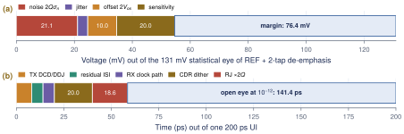
Both budgets close (Figure 14.3). In voltage, REF with only the 2-tap TX de-emphasis leaves a 131 mV statistical eye at \(10^{-12}\); noise (\(2Q\sigma_\mathrm{n}=21\) mV), jitter (3.5 mV), offset (10 mV) and sensitivity (20 mV) leave a 76 mV margin by linear addition, 89 mV statistically (Section 4.4), and the full partition (\(-6\) dB preset + 2-tap DFE, 172 mV noise-free PRBS7 eye, Section 8.5) only adds to it. In time, 40 ps of DJ plus \(2Q\times1.32\) ps of RJ give TJ = 58.6 ps = 0.293 UI, just inside 0.3 UI (Section 11.5). Timing is the tighter budget, and its largest line is the CDR’s own dither.
14.4Design for 10, guarantee 5
Everything so far describes the 5 Gb/s baseline that the rest of this book derives. Can the same architecture go faster? The transistors are not what stops it: a 100 ps UI still holds about fifty SG13G2 CML gate delays (Figure 1.6), while 130 nm CMOS ran out of margin at 5 Gb/s. The limits are the channel, the clocks and the timing budget. This section shows that 10 Gb/s NRZ fits the same architecture with six changes, and sets the project target accordingly: design every high-speed block for 10 Gb/s, and keep 5 Gb/s over REF as the pass criterion of first silicon. The 10 Gb/s column of Table 14.2 collects the resulting numbers.
The equalizer sees decibels, not bits per second
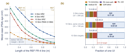
Figure 14.4(a) repeats the partition study of Section 8.5 at 5, 8 and 10 Gb/s NRZ and at 10 Gb/s PAM4, with the CTLE poles moved to each Nyquist frequency. Over REF, 10 Gb/s NRZ meets \(-30.1\) dB at 5 GHz and the worst-case eye closes to 18 mV. Over half the line, 0.5 m with the same pads, it opens to 193 mV, more than the 134 mV of the 5 Gb/s baseline over REF. We call this channel REF-10: \(-15.3\) dB at 5 GHz. The rule behind it is simple. The equalizer only sees the loss at Nyquist; two links with the same loss need the same equalizer, whatever their bit rates. PAM4 at 10 Gb/s keeps the 2.5 GHz Nyquist frequency of REF but gives up two-thirds of each sub-eye: 14 mV over REF and 97 mV over REF-10, below NRZ at both lengths and with three slicers per sample (Section 4.5).
Six changes
The block diagram of Figure 14.1 stays: half-rate clocking, the CMOS/CML split, FFE + CTLE + DFE, a PI-based bang-bang CDR. Six things change.
Clocks at 5 GHz. The half-rate clock doubles. A 10 GHz LC VCO followed by a CML \(\div2\) gives I and Q at 5 GHz, with the quadrature set by the divider rather than by matching (Section 12.5). A second \(\div2\) gives the 2.5 GHz I and Q of the 5 Gb/s mode, so one register selects the rate and the polyphase filter goes away. The cost: the team’s 2.4 GHz PLL [9] is reused for its loop and its flow, not for its tank.
The timing budget. Jitter set in picoseconds does not shrink with the UI. Worked Example 14.1 shows that the budget closes only if those terms roughly halve; this is the main extra work.
One more CML stage on each side. CMOS stays at 1.25 Gb/s per lane or less (Section 9.2). The TX becomes CMOS 16:8 on a 625 MHz word clock, then CML 8:4, 4:2 and the half-rate 2:1; the RX adds one CML 1:2 in front of the CMOS deserializer.
DFE tap 1 is unrolled. The direct tap-1 loop needs about 140 ps (Section 8.2), more than the 100 ps UI, so tap 1 becomes speculative, the fallback already listed in Table 14.2. Each data phase gets two samplers.
Pad and package. For 10 dB of return loss at 5 GHz the pad may carry only half the capacitance, 0.42 pF, and a bond wire only half the inductance, about 0.5 mm (Worked Example 14.2). The T-coil of Section 9.6 stops being a fallback and becomes part of the pad.
Power. CML draws its tails whatever the rate, so only the additions cost power: the extra CML stages, faster clock buffers, two more samplers and the dividers add about 65 mW. That gives \(\approx\)280 mW, or about 28 pJ/b at 10 Gb/s against 43 pJ/b at 5 Gb/s.
Worked Example 14.1 · Does the timing budget close at 10 Gb/s?
Given: the 5 Gb/s budget of Section 11.5: TX DCD/DDJ 8 ps, residual ISI 6 ps, RX clock path 6 ps, CDR dither 20 ps; RJ \(\sigma\) = 1.32 ps (RSS of 1.0, 0.7 and 0.5 ps); \(2Q\) = 14.07 at \(10^{-12}\); target TJ \(\le0.3\) UI.
Same circuits at 10 Gb/s: residual ISI and CDR dither scale with the UI (3 and 10 ps); duty-cycle error, clock-path jitter and RJ are set in picoseconds and stay. DJ = 8 + 3 + 6 + 10 = 27 ps; \(2Q\sigma\) = 18.6 ps; TJ = 45.6 ps = 0.46 UI. The budget fails.
Targets: duty-cycle correction to DCD + DDJ \(\le\) 4 ps, clock path \(\le\) 3 ps, CDR dither \(\le\) 8 ps give DJ = 18 ps. Then \(2Q\sigma \le 30 - 18 = 12\) ps, so \(\sigma\le\) 0.85 ps rms, for example 0.5 ps from the PLL, 0.5 ps from the clock path and 0.45 ps from the TX (RSS 0.84 ps).
Result: at 10 Gb/s every jitter source specified in picoseconds must roughly halve. That is why the PLL row of Table 14.2 asks for 0.5 ps rms at 10 GHz, and why Figure 14.4(b) shows timing, not the eye height, as the 10 Gb/s problem.
Why not 25 Gb/s?
SiGe BiCMOS of this class has been used for clock recovery at far higher rates. But past about 12 Gb/s over these channels the architecture changes: a quarter-rate or all-CML datapath with eight calibrated clock phases, more DFE taps with adaptation, clocks below 300 fs rms, flip-chip or a better package, and channels under about 25 cm. That is a different chip and a larger team, so it belongs to Phase 4 of Section 14.8.
14.5From transceiver to test chip
Figure 14.1 is the transceiver. To measure it, the transceiver must sit on a die with test logic around it, a floorplan that respects its three boundaries, and a package that does not ruin its 2.5 GHz signals. This section shows the concept for each. The details will change as the blocks are designed, but the rules behind them will not.
14.5.1The test chip
Figure 14.5 is the chip-level view of Figure 14.1, with the test logic made explicit. Digital blocks sit on the left: SPI configuration registers that reach every block, a PRBS7/31 generator for the TX, and a PRBS checker with an error counter for the RX. The TX row runs across the top (serializer, 3-tap FFE, CML driver), and the RX row runs back along the bottom (CTLE, sampler with DFE, deserializer). The LC-PLL takes an external reference and clocks the TX; the CDR steers the sampling phase from the data itself. Two paths close the loop. The internal loopback sends the driver output straight to the RX input, which tests the whole chip with no board at all. The external path goes through a test PCB, SMA cables and trace coupons, which adds a real channel.
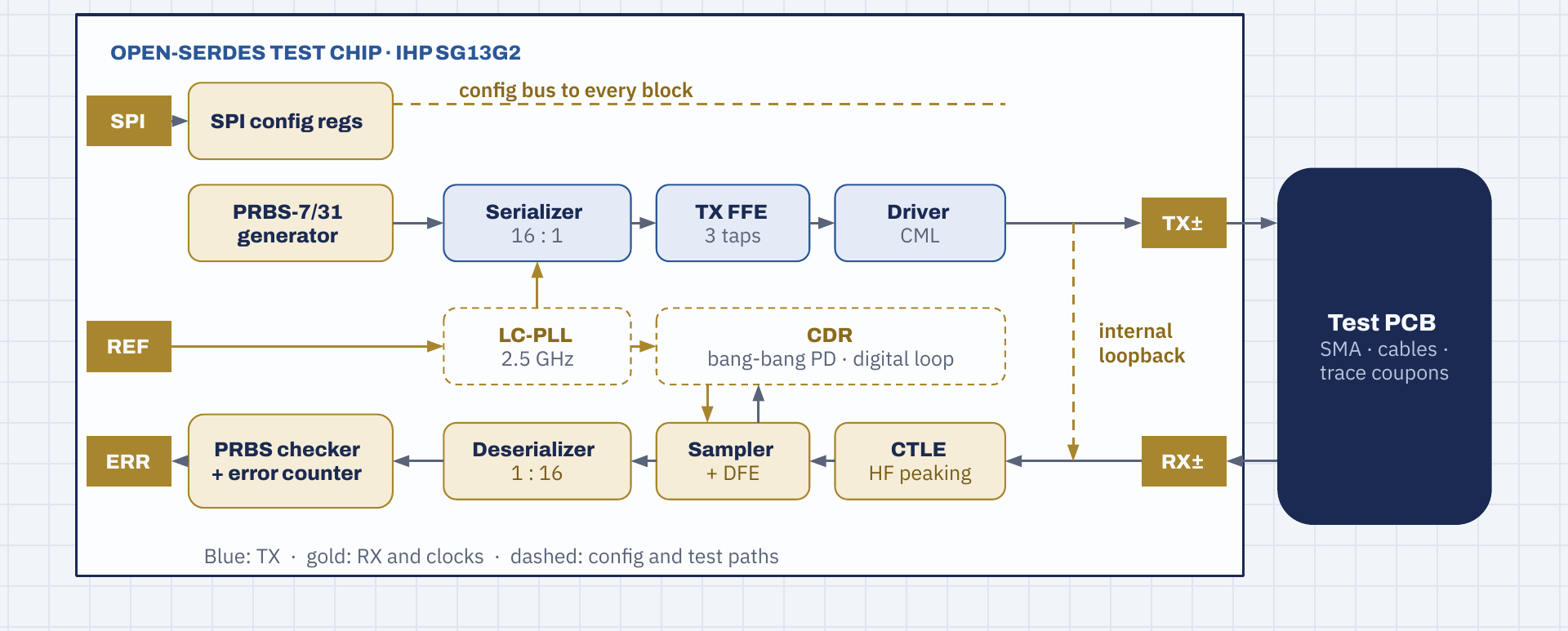
The error counter is what makes a cheap lab possible. With PRBS31 running and the counter at zero, a BER below \(10^{-12}\) is shown at 95 % confidence after \(3/\mathrm{BER} = 3\times10^{12}\) bits, which takes 10 minutes at 5 Gb/s (Section 15.5). An oscilloscope then only has to show the eye, not count errors.
14.5.2Floorplan
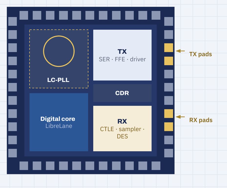
Figure 14.6 is a first floorplan. Each placement follows from a number in an earlier chapter:
TX and RX pads on one edge, so the high-speed bond wires are the shortest on the die (Worked Example 14.2).
The LC-PLL in its own corner, with a guard ring and its own supply, away from the switching digital core. The 4 nH inductor needs keep-out space on TopMetal2 (Section 15.4).
TX and RX next to their pads, with the CDR between them, because the I/Q clocks and the PI outputs must reach four samplers with matched delays (Section 12.5).
Three supply domains: AVDD at about 2.5 V for the HBT CML, DVDD at 1.2 V for CMOS, and VDDIO at 3.3 V for the pads. This is the supply boundary of Section 14.2, drawn on silicon.
A digital core hardened with LibreLane, and the seal ring, fill and logo taken from the JKU template flow [5].
The die is about \(2\times2\) mm\(^2\) for now. The PLL alone is 0.347 mm\(^2\) [9], and the final size waits for the block layouts.
14.5.3Package and pinout
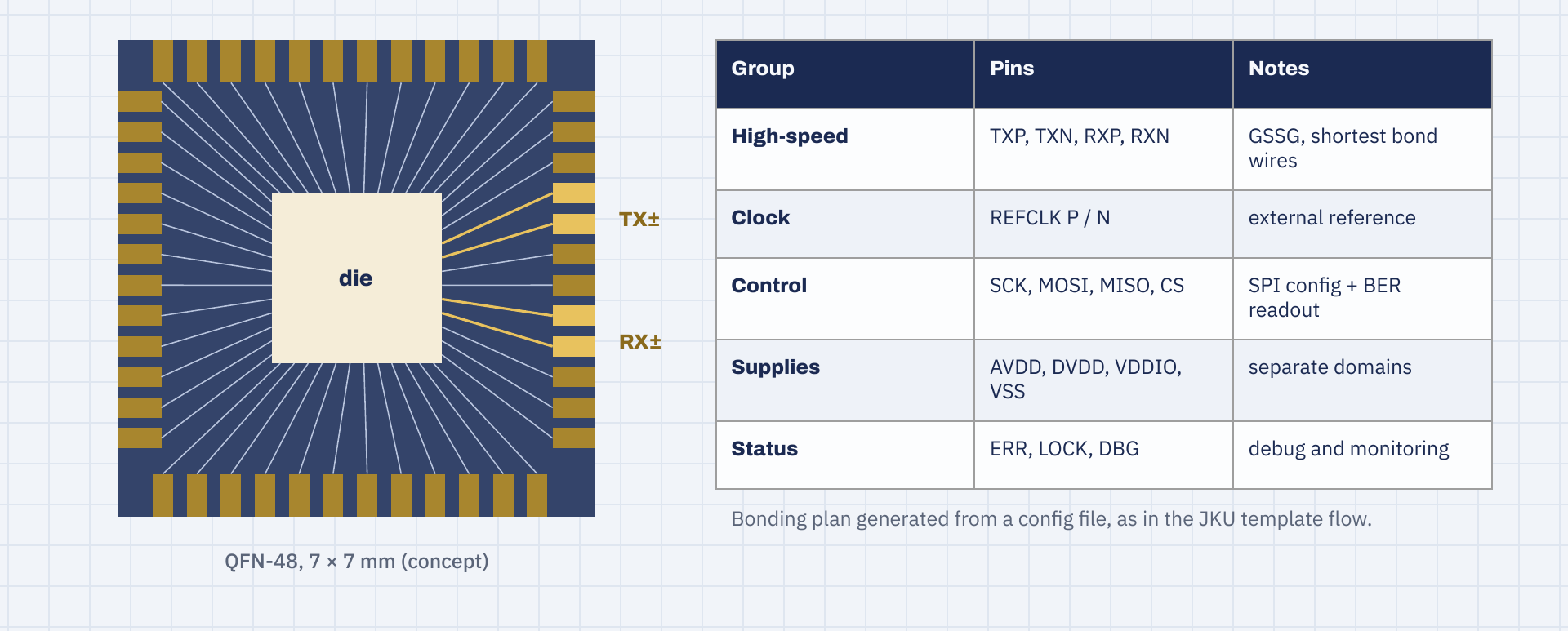
A QFN package is cheap and easy to solder to a test PCB, but every bond wire is a series inductor of about 1 nH per millimeter (Worked Example 3.4). Figure 14.7 shows a QFN-48 concept: the four high-speed pins on one side, with ground pins between them (GSSG), and the clock, SPI, supply and status pins grouped around the rest. As in the JKU template, the bonding plan is generated from a configuration file, so a pin change is one edit.
Worked Example 14.2 · How long may a high-speed bond wire be?
Given: a bond wire of \(L \approx 1\) nH per mm in series between two 50 Ω environments; a return-loss goal of 10 dB at \(f_\mathrm{N}= 2.5\) GHz, the same goal as for the pad in Table 14.2.
Return loss of a series inductor: with \(x = \omega L/(2Z_0)\), \(\lvert S_{11}\rvert = x/\sqrt{1+x^2}\) (Worked Example 3.4).
1 mm, 1 nH: \(x = 2\pi\cdot2.5\,\mathrm{GHz}\cdot1\,\mathrm{nH}/100\,\Omega = 0.157\), so \(\lvert S_{11}\rvert = 0.155\) and RL = 16.2 dB.
2.5 mm, 2.5 nH: \(x = 0.393\), so RL = 8.7 dB. This already misses the goal, before the pad capacitance is added.
3 mm, 3 nH (a corner pad of a large QFN): RL = 7.4 dB.
At 5 GHz, the Nyquist frequency of the 10 Gb/s target (Section 14.4), 1 mm gives \(x = 0.314\) and RL = 10.5 dB, with nothing left for the pad; 0.5 mm gives 16.2 dB again.
Result: keep the high-speed bond wires at or below about 1 mm, and about 0.5 mm for the 10 Gb/s target. That rule puts the TX and RX pads on the die edge closest to their package pins, and puts those pins in the middle of one package side. If the wires cannot be that short, part of the inductance can be absorbed into the T-coil of Section 9.6.
14.6Power budget
A CML gate draws its tail current whatever the data, so a CML-heavy chip has a power budget you can write down before any layout: list the tails, multiply by the supply. CMOS logic burns \(\alpha C V^2 f\) instead.
Key equation · CML power and energy per bit
\[P_\mathrm{CML} = V_\mathrm{CC}\sum_i I_{T,i},\qquad P_\mathrm{CMOS}=\alpha\,C_\mathrm{sw}V_\mathrm{DD}^2f,\qquad E_b = \frac{P_\mathrm{total}}{f_\mathrm{b}} \tag{14.2}\]
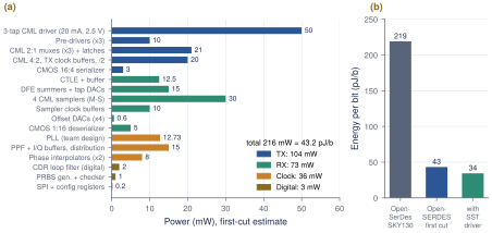
Table 14.3 collects the estimates of Chapters 9, 10, 12 and 13 and Figure 14.8 plots them. Assumptions: 1 Vppd swing (20 mA driver tail); CML gates as in Worked Example 9.3, about 1.2 mA each with emitter followers; CML on 2.5 V, CMOS on 1.2 V; the team’s measured PLL power of 12.73 mW [9]. The polyphase buffers, the PIs and the sampler clock buffers are separate circuits and are counted separately.
| Blocks | Assumption | mW | |
|---|---|---|---|
| TX | 3-tap CML driver | \(I_T\) = 20 mA from 2.5 V (40 mW at 0.8 Vppd) | 50.0 |
| CML 4:2, 2:1 (\(\times3\)), latches, pre-drivers, clock buffers, \(\div2\) | about 17 CML gates of 1.2 mA | 51.0 | |
| CMOS 16:4 | 1.2 V, 625 MHz | 3.0 | |
| RX | CTLE + buffer, DFE summers and tap DACs | 5 mA + 6 mA | 27.5 |
| 4 CML samplers + their clock buffers | 12 mA + 4 mA | 40.0 | |
| CMOS 1:16 deserializer, offset DACs | 1.2 V; 5 bits \(\times4\) | 5.6 | |
| Clocking | PLL (team design) | measured, 130 nm BiCMOS [9] | 12.7 |
| polyphase + I/Q buffers, distribution, 2 PIs | 6 mA + 8 mW (Section 13.6) | 23.0 | |
| Digital | CDR loop filter, PRBS gen. + checker, SPI | CMOS at 625 and 312.5 MHz | 3.2 |
| Total | TX 104, RX 73, clocking 36, digital 3 | 216 |
Worked Example 14.3 · Energy per bit, and where to save
Total: the CML tails add up to 77 mA from 2.5 V (192 mW); the PLL, the CMOS blocks and the DACs add 25 mW: \(P\approx216\,\mathrm{mW}\). By Equation (14.2), \(E_b = 216\,\mathrm{mW}/5\,\mathrm{Gb/s} = \mathbf{43.2}\) pJ/b.
Comparison: the Purdue OpenSerDes spends \(438\,\mathrm{mW}/2\,\mathrm{Gb/s} = 219\) pJ/b [11]. Open-SERDES runs 2.5 times faster for about half the power, five times less energy per bit, because the HBTs do in a few CML gates what an all-digital 130 nm CMOS design must do with oversampling and many more gates.
Savings, largest first: (1) the SST driver of Section 9.4 saves about 44 mW, giving 172 mW and 34.4 pJ/b; (2) a swing of 0.8 Vppd saves 10 mW; (3) each CML gate removed from the clock paths saves about 3 mW. Lowering the CML supply would save the most of all, but every \(V_\mathrm{CE}\) must still fit below \(\mathrm{BV}_\mathrm{CEO}\) with the swing on top (Section 9.4), so this waits for silicon data.
14.7Design decisions
Table 14.4 lists the ten choices that shape Open-SERDES. Each row says what was chosen, what was rejected and why, and where the argument is made in full. Use it in design reviews: if someone proposes to change a row, the chapter in the last column says which numbers must be recomputed.
| Decision | Chosen | Alternatives | Why | Ch. |
|---|---|---|---|---|
| Modulation | NRZ | PAM4 | on REF NRZ wins by 2.6 dB; PAM4 pays only above about 24 dB and needs 3 slicers and linear circuits; at 10 Gb/s NRZ wins at every length | Sections 4.5 and 14.4 |
| Clock rate | half rate: 2.5 GHz at 5 Gb/s, 5 GHz at 10 Gb/s | full rate, quarter rate | full rate doubles every clock; quarter rate needs 8 calibrated phases | Sections 9.2 and 12.5 |
| Fast logic | SiGe HBT CML | CMOS, MOS CML | full switching at 100 mV, gain 5.8 vs. 2; CMOS misses the 8 FO4 rule at 2.5 GHz, slow corner | Section 9.2 |
| TX driver | CML | SST (voltage mode) | resistor-set impedance, constant current, taps leave the impedance alone; SST (\(-44\) mW) is the upgrade | Section 9.4 |
| TX FFE | 3 taps | 2 taps, 4+ taps | post-tap does most of the work; pre-tap for \(p_{-1}\) on longer channels (on REF, 2 taps win: Lab 3) | Chapter 6 and Section 16.4 |
| RX equalizer | CTLE 0–12 dB + 2-tap DFE | CTLE only, more DFE taps, RX FFE | DFE removes \(p_1\), \(p_2\) without noise; CTLE adds gain, adaptivity and reach above 22 dB; tap 1 unrolled at 10 Gb/s | Sections 8.5 and 8.2 |
| VCO | LC: 2.5 GHz baseline, 10 GHz target | ring VCO | 15–30 dB lower phase noise; the team’s proven 2.4 GHz design sets the topology and the flow | Sections 12.4 and 14.4 |
| CDR | PI dual loop, digital BB | VCO-based BB, linear (Hogge) | reuses the clean PLL; synthesizable; PVT-independent gain; no false lock | Section 13.6 |
| Quadrature | baseline: 2-stage polyphase; target: 10 GHz VCO + CML \(\div2\) | quadrature VCO | polyphase keeps the 2.5 GHz VCO; \(\div2\) gives exact I/Q at both rates and a second \(\div2\) selects the rate | Sections 12.5 and 14.4 |
| On-chip test | PRBS7/31 + checker, loopback | external BERT only | scope and PC suffice; \(10^{-12}\) in 10 minutes; loopback isolates the chip | Section 15.5 |
14.8Roadmap: from blocks to silicon
Open-SERDES is built in five phases (Figure 1.5). Each phase ends with a tagged release of design files, models and data, and each must prove something specific before the next one starts. Table 14.5 states what that is.
| Phase | Work | Exit criterion and release | Chapters |
|---|---|---|---|
| 0 · Feasibility | channel and link model; pick the architecture; freeze block specs | the link, TX and RX rows of Table 14.2 confirmed in simulation; REF replaced by a standard channel; release: model + spec file | Chapters 3, 4 and 8 |
| 1 · Building blocks | HBT/CML cell library sized for 10 Gb/s; driver, CTLE, sampler, and the 10 GHz VCO with its \(\div2\); a test-chip shuttle (Tiny Tapeout [43] IHP or an IHP open MPW) | measured CTLE \(H(f)\), driver eye, sampler offset and sensitivity, and VCO phase noise back in the model; release: cell library + block GDS | Chapters 7, 9, 10 and 12 |
| 2 · 5/10 Gb/s transceiver | TX + RX + PLL + CDR with a rate select; on-chip PRBS loopback; full-chip tape-out | post-layout statistical eye meets the pass criteria at 5 Gb/s over REF (required) and at 10 Gb/s over REF-10 (target); full-chip DRC/LVS clean; release: GDSII + RTL | Chapters 12, 13 and 15 and Section 14.4 |
| 3 · Measure and publish | test PCB; eye and BER in both modes; open measurement data; paper (IEEE JSSC or TCAS, SMACD 2027) | BER \(\le10^{-12}\) at 5 Gb/s through a real channel and at 10 Gb/s through a short one; bathtub and JTOL measured; release: data + paper | Section 15.5 and Chapter 16 |
| 4 · Beyond | 16–25 Gb/s (quarter-rate or all-CML datapath); adaptive DFE; PAM4 for lossy channels; multi-lane and chiplet links | a new spec table, starting from the measured Phase-3 data | Sections 4.5, 8.3 and 14.4 |
Why Phase 1 comes before the full chip
Every \(^\dagger\) in Table 14.2 is a risk until it is measured. A small shuttle with only the driver, the CTLE, the samplers and the 10 GHz VCO turns the riskiest estimates (pad capacitance, CTLE peaking, sampler offset, phase noise at 10 GHz) into data a year before the full chip, while the PLL loop and the CDR logic can rely on the team’s existing PLL and on simulation.
14.9Risks and open questions
The architecture closes on paper. It can still fail in these places, roughly in order of the cost of a late fix:
ESD and pad capacitance. ESD diodes can take most of the 0.85 pF budget alone; get the SG13G2 ESD cell capacitance early, and keep the T-coil of Section 9.6 as the fallback.
\(\mathrm{BV}_\mathrm{CEO}\) headroom. The off driver transistor sits at 1.25–1.5 V against about 1.6 V; simulate every \(V_\mathrm{CE}\) at every corner with the real termination.
PLL phase noise. The quoted \(-100.8\) dBc/Hz at 1 MHz is far worse than Leeson predicts (Section 12.4); the 1 ps RJ line depends on what it really is.
Inductor EM modeling. The 4 nH tank and any T-coil must be EM-simulated on TopMetal2 (Section 15.4) and matched to the team’s measured \(Q\).
Timing loops. DFE tap 1 uses about 140 of its 200 ps and the CDR dither 19 of its 20 ps; both need post-layout confirmation.
The 10 GHz clock and the 10 Gb/s timing budget. The VCO is a new design, and the budget needs every picosecond term roughly halved (Worked Example 14.1). Put the VCO and its \(\div2\) on the Phase-1 shuttle, and give the test chip an external clock input so that both modes can be measured without the on-chip PLL.
Packaging and measurement. Bond wires longer than about 1 mm (0.5 mm at 10 Gb/s) cost return loss (Worked Example 14.2); the test PCB, a clean reference clock and access to a sampling scope or BERT must be ready before first silicon.
Area, pads and the channel. The PLL is 0.347 mm\(^2\) [9], the MIM capacitors add tenths of a mm\(^2\), and the high-speed pads need SMA-grade access; REF must be replaced by measured S-parameters (Section 16.9).
Key takeaways
Open-SERDES delivers six things: the GDSII, the RTL and benches, the link model and GUI, an HBT/CML cell library, documentation, and a paper with open data.
Open-SERDES is a single-lane transceiver: CMOS at 312.5 MHz in the core, HBT CML at 1.25 GHz and above, joined by level converters, two supplies and two clock domains.
One 2.5 GHz LC PLL feeds both sides: the TX divides it; the RX makes four phases and rotates them in 6.25 ps steps under digital CDR control.
The block specification table is the contract: every block has a 5 Gb/s and a 10 Gb/s number and a chapter; \(^\dagger\) marks estimates awaiting simulation.
Design for 10, guarantee 5: the same architecture carries 10 Gb/s NRZ over 0.5 m of FR-4 (193 mV worst-case eye) because the equalizer only sees the loss at Nyquist. The work is in the clocks and the timing budget (RJ \(\le0.85\) ps rms), not in the transistors.
The voltage budget leaves about 76 mV; the timing budget leaves a 141 ps eye with 1.4 ps to spare.
The test chip adds SPI, a PRBS generator and checker with an error counter, and an internal loopback; TX and RX pads share one die edge, and high-speed bond wires stay at or below about 1 mm.
Five phases, each with an exit criterion and a tagged release: feasibility, building blocks, the 5/10 Gb/s transceiver, measurement, and beyond.
First-cut power is about 216 mW (43 pJ/b), five times less energy per bit than OpenSerDes, dominated by static CML current; the SST driver is the first saving.
Generated from book/tutorial/chapters/14_arch.tex. Figure, table and equation numbers match the PDF edition.