Chapter 1Why Serial Links?
Chips have far more bandwidth inside than pins to move it out, so we send bits one after another, very fast, over a few carefully engineered wires.
In this chapter you will learn
explain why high-speed I/O moved from wide parallel buses to serial links with an embedded clock;
name every block of a SerDes link and the data rate at each point of the Open-SERDES design;
place 5 Gb/s NRZ among real standards such as PCIe, USB and backplane Ethernet;
state the Open-SERDES targets and why 5 Gb/s NRZ in SG13G2 is the right first chip;
compare the speed of SG13G2 HBTs with 130 nm CMOS, and describe the back-end metal stack.
1.1From parallel buses to serial links
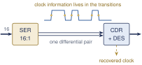
The obvious way to move data between chips is a parallel bus: one wire per bit plus a clock wire. A 16-bit bus at 312.5 Mb/s per wire moves 5 Gb/s. As rates grew, four problems stopped it from scaling (Figure 1.1a).
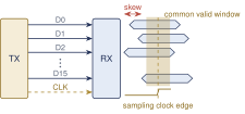
Skew. Lanes differ in length, load and driver strength, so bits launched together arrive at different times; the usable window is the bit time minus the worst skew.
Pin count. Pins and board area are expensive and grow far more slowly than on-chip bandwidth, and a wide bus needs many return pins.
Power and noise. Many single-ended drivers switching together cause supply bounce and crosstalk, and the energy per bit stays high.
The clock wire. The forwarded clock must be matched to every lane across process, voltage and temperature.
A serial link serializes the word into one full-rate stream on a single differential pair, which carries its own return path and rejects common-mode noise. No clock is sent: a clock and data recovery (CDR) circuit in the receiver locks a local clock to the data transitions, so the clock is embedded in the data and lane-to-lane skew no longer matters.
Worked Example 1.1 · Skew budget: parallel bus versus serial link
A signal on FR-4 (\(\varepsilon_r \approx 4\)) travels at \(v = c/\sqrt{\varepsilon_r} \approx 0.15\,\mathrm{mm}/\mathrm{ps}\), or about 6.7 ps per millimeter. Suppose two lanes differ in length by 10 mm, a modest mismatch on a crowded board. The skew is \(10\,\mathrm{mm}\times6.7\,\mathrm{ps}/\mathrm{mm} \approx 67\,\mathrm{ps}\).
16-bit bus at 312.5 Mb/s: the bit time is 3.2 ns, so the skew costs \(67/3200 \approx 2\%\) of it.
The same bus pushed to 5 Gb/s per lane: the bit time is 200 ps and the same skew eats one third of it, before any jitter or noise.
The pins tell a similar story: 16 data wires plus a clock and their returns, against one differential pair (2 pins) for the serial link.
The price is speed: each bit lasts only \(T_\mathrm{b}= 1/f_\mathrm{b}\), and the wire that looked ideal at 312.5 Mb/s now smears each bit into its neighbors. Paying that price efficiently is measured by the energy per bit.
Key equation · Energy efficiency of a link
\[E_b = \frac{P_\mathrm{link}}{f_\mathrm{b}}, \qquad 1\,\mathrm{mW} \text{ per } \mathrm{Gb}/\mathrm{s} = 1\,\mathrm{pJ}/\mathrm{b} \tag{1.1}\]
A transceiver burning 50 mW at 5 Gb/s spends 10 pJ per bit.
What this means for your design
Serial links win because they trade many slow, skew-limited wires for one fast, self-clocked wire. The cost moves into the transceiver: it must drive, equalize and re-time a 200 ps bit after a lossy channel. Every chapter that follows is about doing that within a power budget.
1.2Anatomy of a SerDes link
Figure 1.2 shows the complete Open-SERDES link. Follow a 16-bit word from left to right.
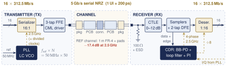
Transmitter (TX)
The serializer works in stages: CMOS logic does 16:4, current-mode logic (CML) does 4:2, and a half-rate 2:1 CML multiplexer clocked at 2.5 GHz emits one bit per clock edge (Section 9.2). The driver launches a 1 Vppd signal into the 50 Ω-per-side channel through a 3-tap feed-forward equalizer (FFE) that pre-distorts it against the channel loss (Chapter 6 and Section 9.4). A phase-locked loop (PLL) with an LC oscillator makes the 2.5 GHz clock (Chapter 12).
Channel
Packages, board (PCB) traces and vias and a connector together act as a low-pass filter with reflections; the Open-SERDES reference channel loses 17.4 dB at 2.5 GHz (Chapter 3).
Receiver (RX)
A 100 Ω termination with ESD protection absorbs the wave (Section 9.3). A continuous-time linear equalizer (CTLE) restores the lost high frequencies (Chapter 7). Four samplers on the 0°/90°/180°/270° phases of a 2.5 GHz clock take data and edge samples, while a 2-tap decision-feedback equalizer (DFE) subtracts the echo of previous bits (Chapter 8 and Section 10.2). The CDR steers a phase interpolator to keep the samples centered (Chapter 13), and the deserializer rebuilds the 16-bit word (Section 10.6).
Worked Example 1.2 · Following the rates through the link
Parallel side: \(16 \times 312.5\,\mathrm{Mb}/\mathrm{s} = 5000\,\mathrm{Mb}/\mathrm{s} = 5\,\mathrm{Gb}/\mathrm{s}\).
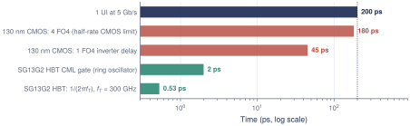
Serial side: \(T_\mathrm{b}= 1/5\,\mathrm{Gb}/\mathrm{s} = 200\,\mathrm{ps}\), the unit interval (UI).
Half-rate clock: 2.5 GHz has a 400 ps = 2 UI period; both edges give one bit per 200 ps. The four CDR phases are 0.5 UI apart: two data centers and two edges.
PLL: \(f_\mathrm{ref} \times N = 50\,\mathrm{MHz}\times 50 = 2.5\,\mathrm{GHz}\). The deserializer output clock is \(2.5\,\mathrm{GHz}/8 = 312.5\,\mathrm{MHz}\).
The half-rate clock frequency equals the Nyquist frequency \(f_\mathrm{N}= f_\mathrm{b}/2\) of the data (Section 2.1).
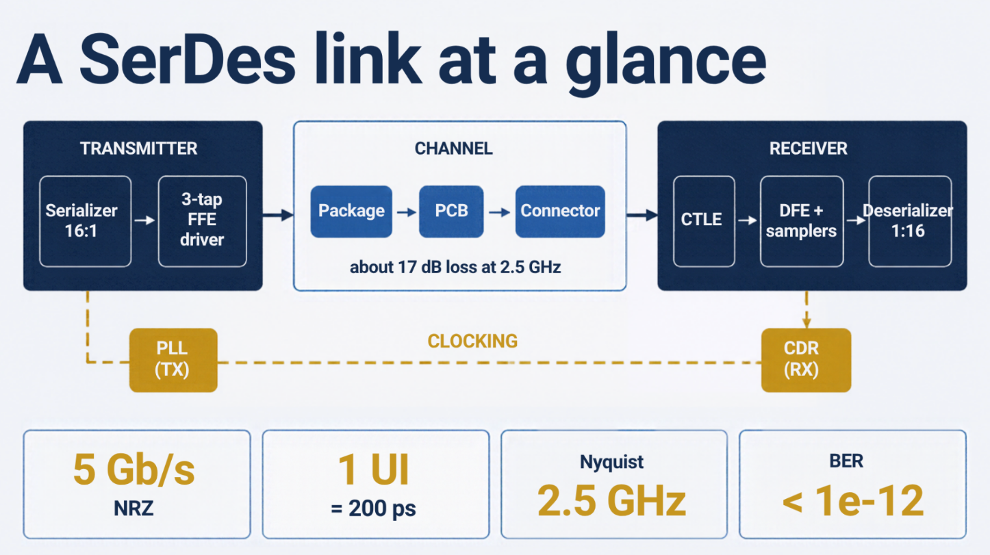
Figure 1.3 summarizes the link with the four numbers you will meet on almost every page.
1.3Where SerDes are used
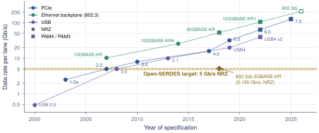
Serial links connect a CPU to its graphics card (PCIe), a computer to its drives (USB, SATA) and the line cards of a network switch (Ethernet). Table 1.1 lists common standards. GT/s counts symbols on the wire and Gb/s counts bits; they are equal for NRZ, while PAM4 carries two bits per symbol (Section 4.5). Line rates include coding overhead: 8b/10b sends 10 line bits per 8 data bits, 64b/66b sends 66 per 64.
| Standard (year) | Rate per lane | Modulation and coding | \(f_\mathrm{N}\) (GHz) |
|---|---|---|---|
| PCIe 1.0a / 2.0 (2003 / 2007) | 2.5 / 5 GT/s | NRZ, 8b/10b | 1.25 / 2.5 |
| PCIe 3.0 / 4.0 / 5.0 (2010–19) | 8 / 16 / 32 GT/s | NRZ, 128b/130b | 4 / 8 / 16 |
| PCIe 6.0 (2022) | 64 GT/s | PAM4, 32 GBd, FEC | 16 |
| USB 3.2 Gen 1 / Gen 2 (2008 / 2013) | 5 / 10 Gb/s | NRZ, 8b/10b / 128b/132b | 2.5 / 5 |
| USB4 v2 (2022) | 40 Gb/s | PAM3, 25.6 GBd | 12.8 |
| SATA I / II / III (2003–09) | 1.5 / 3 / 6 Gb/s | NRZ, 8b/10b | 0.75 / 1.5 / 3 |
| 2.5GBASE-KX (802.3cb, 2018) | 3.125 Gb/s | NRZ, 8b/10b | 1.56 |
| 5GBASE-KR (802.3cb, 2018) | 5.156 Gb/s | NRZ, 64b/66b | 2.58 |
| 10GBASE-KR (802.3ap, 2007) | 10.3125 Gb/s | NRZ, 64b/66b | 5.16 |
| 100GBASE-KR4 (802.3bj, 2014) | 25.78 Gb/s | NRZ, RS-FEC | 12.9 |
| 400GBASE-KR4 (802.3ck, 2022) | 106.25 Gb/s | PAM4, 53.1 GBd, FEC | 26.6 |
| UCIe 1.0–3.0 (2022–25) | 4–64 GT/s | NRZ, single-ended, fwd. clock | \(\le\) 32 |
The last row is a useful counterexample: UCIe links chiplets millimeters apart in one package, where thousands of short, matched wires are cheap, so the parallel bus with a forwarded clock wins again. Serial links win when the wire is long, lossy and expensive, which is the situation Open-SERDES targets.
Figure 1.4 shows per-lane rates doubling roughly every three to four years. Around 50 Gb/s the industry moved to PAM4, because the loss at the NRZ Nyquist frequency became too high.
1.4The Open-SERDES project
Open-SERDES is an open project to design a complete 5 Gb/s serial-link IP for Ethernet-class backplane links in IHP SG13G2, using only open-source PDKs and tools, with every schematic, layout, model and test bench public. The scope runs from specifications and architecture, through a Python link-simulation framework, to the circuits, custom analog layout, synthesized and routed digital blocks, and post-layout verification with DRC and LVS. The deliverables are a tape-out-ready GDSII, Verilog RTL with test benches, a demonstration of the modeling framework, a documented GitHub repository with a thesis, and a paper on the whole flow. The specnote collects the targets; Chapter 14 expands them.
Open-SERDES target (reference design)
| Data rate | 5 Gb/s NRZ, \(T_\mathrm{b}= 1\,\mathrm{UI}= 200\,\mathrm{ps}\), \(f_\mathrm{N}= 2.5\,\mathrm{GHz}\) |
| Target BER | \(\le 10^{-12}\) (\(Q = 7.03\)); PRBS7 for bring-up, PRBS31 for compliance |
| Channel | REF: 1 m FR-4 stripline + 300 fF pads, −17.4 dB at 2.5 GHz |
| TX | 16:1 serializer (half-rate 2:1 CML mux), HBT CML driver, 3-tap FFE, 1 V\(_\mathrm{ppd}\), 100 Ω diff. |
| RX | 100 Ω termination + ESD, HBT CTLE (0–12 dB), half-rate 2-tap DFE, 4 samplers, 1:16 deserializer |
| Clocking | integer-\(N\) CP-PLL, LC VCO at 2.5 GHz (\(f_\mathrm{ref}\) = 50 MHz, \(N\) = 50); PI-based bang-bang CDR, 64 PI steps per 2 UI |
| Test | on-chip PRBS7/31 generator and checker, near-end loopback |
Why 5 Gb/s NRZ is the right first target
Fast enough to be real. It matches PCIe 2.0, USB 3.2 Gen 1 and 5GBASE-KR, and a 1 m board loses 17 dB at 2.5 GHz: the raw eye is closed, so every equalization idea in this book is needed.
Slow enough to be safe. A 200 ps UI is easy for SG13G2 HBTs but at the edge of 130 nm CMOS (Section 1.5), which shows clearly why BiCMOS helps.
NRZ is simple and robust. PAM4 costs about 9.5 dB of eye, three times the samplers and better linearity, which pays off only on much lossier channels (Section 4.5).
Proven blocks. The team’s 2.4 GHz LC-VCO PLL in 130 nm BiCMOS [9] moves to 2.5 GHz with little change.
Prior art
A previous undergraduate project modeled a 5 Gb/s SerDes in a commercial 28 nm library [10]. The Purdue OpenSerDes [11] was the first open-source SerDes: an all-digital, synthesizable SkyWater 130 nm CMOS design with inverter-based drivers and an oversampling CDR. In post-layout simulation it ran at 2 Gb/s and drew about 438 mW, mostly in the serializer, deserializer and CDR logic; standard 130 nm CMOS cells capped its speed. Neither project produced a silicon-proven, open, analog 5 Gb/s SerDes. Open-SERDES keeps OpenSerDes’s open flow but moves the fastest circuits to SiGe HBTs, which breaks the CMOS speed limit at the same 130 nm node.
The plan
We organize the scope into five phases (Figure 1.5): specifications, channel and supply plan (Phase 0); the serdespy system model that checks every later decision (Phase 1); circuits and digital RTL (Phase 2); layout, place-and-route, extraction and EM simulation (Phase 3); and sign-off, tape-out and lab test (Phase 4).

1.5IHP SG13G2 at a glance
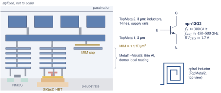
SG13G2 is IHP’s 130 nm SiGe:C BiCMOS process, and its PDK is open source [1]. It offers two kinds of transistor on one die: standard 130 nm CMOS (1.2 V thin-oxide core devices and 3.3 V thick-oxide I/O devices), and the npn13G2 SiGe heterojunction bipolar transistor (HBT), with \(f_T \approx 300\,\mathrm{GHz}\) and \(f_{max} \approx\) 450–500 GHz [12].
HBT versus CMOS speed
The transit frequency \(f_T\), where the current gain falls to one, sets the device’s intrinsic time scale \(1/(2\pi f_T)\): about 0.5 ps for the HBT. A 130 nm NMOS peaks on the order of 100 GHz, and only at its best bias, and logic gates never operate there. A better yardstick for logic is the FO4 delay, the delay of an inverter driving four copies of itself: about 45 ps in 130 nm CMOS. Figure 1.6 puts these times next to the 200 ps UI.
Why CML with HBTs
The fast blocks (final mux, driver, CTLE, samplers, clock buffers) use current-mode logic: a differential pair steers a constant tail current into one of two load resistors. The swing is small (a few hundred millivolts), the supply current is constant, so little switching noise is injected, and an HBT pair switches fully with only about \(4V_T \approx 100\,\mathrm{mV}\) of input, because \(g_\mathrm{m}= I_C/V_T\) is several times a MOSFET’s per unit current (Sections 9.4 and 7.4).
The back end
SG13G2 has seven aluminum metal layers (Figure 1.7): thin Metal1–Metal5 for dense wiring, and thick TopMetal1 (2 µm) and TopMetal2 (3 µm), whose low resistance suits spiral inductors (LC VCO, inductive peaking), on-chip transmission lines and supply rails. A MIM capacitor of roughly 1.5 fF/µm² (check the PDK) sits below TopMetal1.
Supplies
CMOS logic (slow SER/DES stages, PRBS, digital CDR loop) runs from 1.2 V. HBT CML stacks a load, a switching pair and a tail source, so it uses a separate analog supply, nominally 2.5 V, to be confirmed in Phase 0.
Respect \(BV_{CEO}\)
The npn13G2 breakdown voltage \(BV_{CEO}\) is only about 1.7 V. On a 2.5 V supply, an HBT that sees the whole supply (at power-up, or when a tail source saturates) can break down. Check every \(V_{CE}\) in every corner and transient, not just at the operating point.
What this means for your design
Use HBTs where the UI is short (the last mux stage, the driver, the CTLE, the samplers, the VCO and the clock buffers), and CMOS where the rate is low and density matters (the slow serializer and deserializer stages, the PRBS logic and the CDR filter). Put inductors and long high-speed routes on the thick top metals.
1.6How to use the rest of the book
Chapter 2 builds the vocabulary of links (pulse response, eye, BER), Chapter 3 explains the 17.4 dB channel and Chapter 4 turns pulse responses into link budgets. Part II (Chapters 5, 6, 7 and 8) opens the closed eye with equalization. Part III (Chapters 9 and 10) designs the transmitter and receiver circuits. Part IV (Chapters 11, 12 and 13) handles jitter and clocking. Part V (Chapters 14, 15 and 16) assembles the architecture, runs the open-source flow and provides the labs.
Key takeaways
Parallel buses stop scaling because of skew, pin count and switching noise; a serial link sends one fast differential stream and recovers the clock from the data.
A SerDes link is a serializer, an FFE driver, a lossy channel, a CTLE, samplers with a DFE, a deserializer, a PLL and a CDR.
In Open-SERDES, 16 bits at 312.5 Mb/s become 5 Gb/s NRZ with a 200 ps UI and a 2.5 GHz Nyquist frequency, using a half-rate 2.5 GHz clock.
5 Gb/s NRZ matches PCIe 2.0, USB 3.2 Gen 1 and 5GBASE-KR, and the 17.4 dB reference channel forces real equalization.
The targets are BER \(\le 10^{-12}\) over the REF channel with a 3-tap FFE, a 0–12 dB CTLE, a 2-tap DFE, an LC PLL and a PI-based CDR.
SG13G2 HBTs (\(f_T \approx 300\,\mathrm{GHz}\)) far outrun 130 nm CMOS (FO4 \(\approx\) 45 ps), so the fast blocks use HBT CML; \(BV_{CEO} \approx 1.7\,\mathrm{V}\) limits the stack, and the thick top metals carry inductors and lines.
Generated from book/tutorial/chapters/01_intro.tex. Figure, table and equation numbers match the PDF edition.